Unlocking EPROM cores?
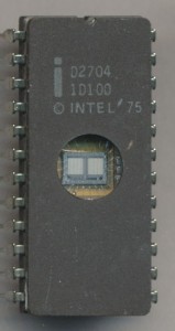
Its well known that manufacturers such as Intel and AMD will sell quad cores as dual cores, or 6-cores as quad-cores in order to meet demand, or to use dies that didn’t ‘make the cut.’ This process has been going on for over 30 years though. Back in the 70’s and 80’s it was very common for a device such as this:
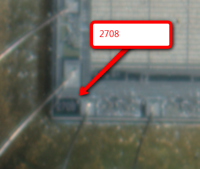
Which is a 2704 4k EPROM, to actually be made from a 2708 die, just with not all the leads connected, or sometimes, with them connected but just labeled as the smaller part. In a production environment, it is cheaper to have a single production line making dies that can be used in more then one device, then having an entire seperate production line just to make a product that may not be the most popular. Look at this die shot (its a bit blurry) but you can see its a 2708 die.
Once again, whats new, really isn’t we have just went from small EPROMs, to CPUs with billions of transistors


July 10th, 2012 at 3:10 am
We are restoring old GRETAG equipment with 8080 from 1978 (!) They were early ! I was looking for the 2704 and 2708 EPROM data sheet from different brands: Signetics and Intel. Maybe it is a good idea for you to add data sheets to your website? Would be lovely to create a good reference for everyone trying to restore old gear like we do. Just a small idea 😉
Cheerio,
Marcus
April 22nd, 2014 at 6:43 pm
[…] by the adding of the 3 to the part number. This certainly was not an uncommon procedure, even Intel regularly sold 2708 EPROMs as 2704s, whether to use a die with an imperfection, or to simply meet […]
September 2nd, 2021 at 9:27 am
I worked for Intel for a summer in the early 1980s and my job was writing production sort test code (code that tests the function of every die on-wafer and implemented any sparing/repair at the same time). If you have a Intel 27128A EPROM, it was tested and possibly “repaired” with my code. That code was entirely 8085A assembly.
For all such products, there were special test modes that are akin today to JTAG test modes but every vendor and every chip implemented it differently back then. Essentially new “personalities and features” were enabled by these test modes. This is how things like sparing were implemented.
Generally you’d raise voltages on pins normally operating at 5V or 12V to particular higher voltage values and that would cause the mode to appear. The functions of the the rest of the pins would change and you could specify taking out half the array (like the 2708 example) or burning in spare rows or columns to replace bad ones in the main array. I don’t remember the specifics for the 27128A – it was too long ago.
The 27128A had 3 spare columns. The 27256A has both spare rows and spare columns (don’t remember how many).
The burning of spares or array block-outs was done with either nichrome fuses, poly fuses or “u-prom” fuses – all of which are nominally irreversible when blown. Which type used depends on the particular generation. The 27128A and later used u-prom fuses.
U-prom fuses are EPROM cells that have an extra metal layer above the device so that UV erase can never erase them when you are erasing the main array. Using them simplifies the process (eliminating an odd-ball and quality/reliability harming nichrome deposition and etch sequence). Polysilicon was fully compatible with an NMOS/CMOS process but had quality/reliability problems. U-prom cells were exactly identical to the product array cells with only a metal mask difference so have the best of all worlds.
This kind of sparing and blocking has always been super common and is still used today in pretty much ALL digital parts to this day. The most common example is N-core processors – there is absolutely no difference in the die between these for a particular family-generation: it’s ONLY about how many of the maximum core count were blocked out (e.g. an 8-core family’s 2-core version is the 8-core with 6 cores blocked either due to failures or due to inventory management).