Intel’s Ivy Bridge: 50 Years of flat transistors come to an end
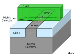
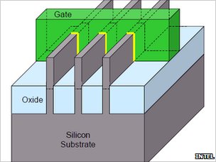
April marked the 50th anniversary of Robert Noyce’s patent on making silicon IC’s with a planar process, a concept that has changed little since then. That is, until this month, when Intel announced their new 22nm process, a process that will not be restricted to planar transistors. Intel, like Hollywood as of late, has gone 3D, Instead of a transistor being built in planes (layers) Intel has developed a way to produce transistors with source/drain spanning several planes on the die, essentially they are formed vertically, rather then horizontally.
This in an of itself is not remarkable, it has been thought of, and done before. What Intel did is make it happen on a commercially viable process. Intel claims to be able to initially manufacture these on a commercial scale at only a 3% cost increase over traditional planar processes, and of course expects that 3% added cost to drop to zero, or in fact result in a cost savings, as the process is refined.
What this allows is 2-3 times the number of transistors in the same space as a planar process (assuming the same process size). Intel plans to use this process for the 22nm node. Intel’s first processor, the 4004, was constructed on a 10 micron process with 2300 transistors. Thats 500,000 times larger features and over a million times less transistors, yet it consumed almost a 1 watt of power. With Intel’s new 3-D 22nm process it should give Intel the break they need into the mobile phone market, a market they have been desiring to reenter ever since selling off their mobile ARM (PXA//StrongARM) division to Marvell several years ago.


