Nvidia GPU Engineering Samples
While we don’t actively collect GPU’s, we do pick them up when they come along, rather then scrap them, and from time to time have been donated a handful of them. Here are a few that have been sitting on my desk that were donated. GPU’s are pretty impressive in their own right (with many having over 1 billion transistors now)
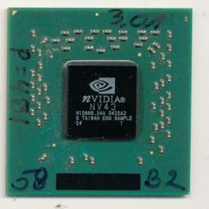
The NV43 is the code name for the Geforce 6600. It was released in August 2004 (abut the time this Engineering Sample was made) and could be clocked at up to 525MHz. It was fab’d by TSMC on a 110nm process and contains 143 million transistors (about the same as a Pentium-M Dothan core).
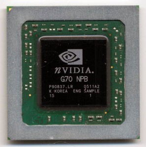
The Nvidia G70 (aka NV47) is the code name for the GeForce 7800 GTX. It was released in June of 2005 and this Engineering Sample was made in March of 2005. It was again made on a 110nm process, containing 302 million transistors @ 550MHz. (A Core 2 Duo has 291 million)
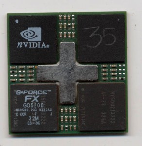
The Nvidia GeForce FX Go 5200 was released in 2003 and was made on a 150nm process with 47million transistors (roughly the same as a P4 Willamette). It was designed for mobile use and as such packaged on a MCM containing the GPU, and in this case, 32MB of DDR.


