August 30th, 2012 ~ by admin

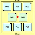
z12 MCM Layout
“We are hitting the limits of physics in many cases” These words, spoken by an IBM engineer about the new zEnterprise EC15 mainframe do well to describe the processor that runs it. The z12, as we’ll refer to this processor, replaces the z196 as IBM’s top performer. The z196 ran at a slothly 5.2GHz, the fastest commercial processor in the world until now. The z12 runs at 5.5GHz and was designed to be clocked up to 6GHz. It is made on a 13layer 32 nm High-K process (the z196 was made on a 45nm process). This allowed a doubling of logic and cache density.
The EC12 is designed with single thread performance in mind. While many systems today focus on massive parallelism, and optimizing code for multi-threading, some tasks do not work well that way, data analytics, batch processing etc, are fundamentally serial processes, so less cores, and more speed per core is far more important. The z12 is based on a MCM (Multi-chip module) that contains 6 Processing Units (PUs) and 2 Storage Controllers (SC, which contain 196MB of L4 cache each) for a total of 8 dies on each MCM. Each PU contains 4, 5 or 6 active cores. The MCM is a 103-layer glass ceramic substrate (size is 96 x 96 mm) containing eight chip sites and 7356 land grid array (LGA) connections.

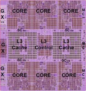
IBM zEC12 6-core PU – 2.75 Billion Transitors – 5.5GHz
Each PU chip has 2.75 billion transistors. Each one of the six cores has its own L1 cache with 64 KB for instructions and 96 KB for data. Next to each core resides its private L2 cache, with 1 MB for instructions and 1 MB for data respectively.
Read More »
August 29th, 2012 ~ by admin

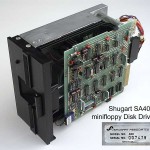
Shugart SA400 Floppy Drive
The HP Input Output Blog has a nice write up on the floppy disk/drive. A very interesting read about a device many took for granted, and many of today’s generation did not ever get to experience. Many do not realize its humble beginnings, and the importance that Steve Jobs, ‘the bum in the lobby,’ played in the 5.25″ floppy becoming a standard. The 5.25″, holding twice what a 8″ floppy could, was developed by Shugart Associated in 1976. Shugart went on to become Seagate, known today for their hard drives. Hard drives that can store over 2 Terabytes of information. The original 5.25″ floppy? 160K, per side. An 8 inch? 80K a side. Interestingly enough, it was sometime before the Floppy Drive Controller (FDC) was integrated onto a single chip. Many original Shugarts used an Intel 8080 CPU for drive processing. The Commodore 64’s famous 1541 Floppy Drive ran its own 6502 type CPU, and was designed in such away you could actually load code directly to the floppy drive 6502. In the 1990’s attempts were made to increase the capacity, speed, and versatility of the floppy. Apple created a 2.88MB 3.5 inch floppy that never really caught on. There was the LS-120 drive which could use normal 1.44MB disks as well as special 120MB disks (was handy, but so few people had them, they had limited use). Ultimately, like most all technology the floppy has passed by the way side, today’s floppy is the USB Flash drive, holding many gigs of data for only a few dollars. And like the floppy, flash drives are used commonly for sneakernetting files around the office. Perhaps the mbile version of the floppy is the Micro-SD card, remember when Sony built a camera with a 1.44MB floppy drive built in? Not een large enough to store the picture from a cell phone camera today.
Head on over and check out the article, its a fascinating story….
August 16th, 2012 ~ by admin
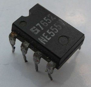
 Yesterday Hans Camenzind passed away at the age of 78. Hans was a notable inventor of Swiss decent. Perhaps the most famous of all his inventions occurred in 1972 while working on a contract with Signetics he invented the 555 Timer chip, a simple oscillating IC that was inexpensive, and easy to build with. Now, even 40 years after its introduction, around a billion per year are still made, by dozens of companies around the world. The 555 Timer is often one of the very first IC’s electronics hobbyist begin experimenting with. Its applications are far reaching and while certainly not a CPU, its significance, and that of Camenzind, should not be forgotten.
The 555 Timer has of course been used in many many computers, notably in the Apple II computer as a joystick controller (558 Timer, which is a quad 555). Other uses include the IBM PC, Ataris, and many many more. In honor of Hans Camenzind, and the 555 Timer, go experiment with one and experience the joys of a device over 40 years old. Dont have one? They cost a whopping $0.95 at Sparkfun.
August 14th, 2012 ~ by admin
The Spacecraft CPU page has been updated, after a long gap. It now includes information of the recently landed Curiosity Lander, some new information on the 45 year old Voyager series as well as some on New Horizons, DAWN, and several others, so check it out.

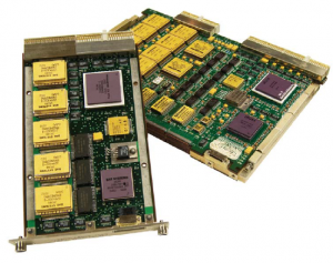
BAE RAD750 Single Board Computers
The Curiosity (and Mars Reconnaissance Orbiter,) Run a BAE RAD750 @ 200MHz


