Archive for February, 2013

February 27th, 2013 ~ by admin

CPU of the Day: Intel 386 Double Stamp

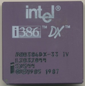
A80386DX-33-SX544DoubleMarkIn coin collecting often times an example is valued not because of its perfection, but because of its imperfections.  An off-center print, the obverse being printed upside down, or the double strike, where a coin doesn’t get cleared form the die and gets hit twice.

Such appears to be the case with this Intel A80386DX-33.  It clearly went through the engraver twice. A similar example (from the same exact lot) is fine, so clearly this one, made in early 1992, was a mistake that was not caught.  I have seen mis-aligned prints, off center etc, but this is the first example i have seen that was engraved twice.  It is interesting that even within the same lot, the spacing of the markings varied somewhat.  Notice that on the right side of the chips the sets of markings line up but they diverge towards the left.  It appears the stepper motors moving the tooling or the chips were a bit sloppy or out of calibration.

Have you seen any other double engraved comments? Let us know in the comments.

Tags:
,

Posted in:
CPU of the Day

February 21st, 2013 ~ by admin

Charles Moore: From FORTH to Stack Processors and Beyond

NRAO Radio Telescope

NRAO Radio Telescope

There are many greats of the CPU industry, some, such as Federico Faggin (designer of the 4004 and worked on the 8008, then founded Zilog) are fairly well known.  Others include Gelsinger and Meyer (of x86 fame) perhaps even Gordon Moore, of which a  ‘law’ is named.  Chuck Peddle and Bill Mensch designed the ubiquitous 6502 processor, but there were more, many more. Engineers whose names have been oft forgotten, but whose work has not.  The 1970’s and 80’s were the fast and the furious of processor designs.  Some designs were developed, sold, or canceled in weeks, months; years were not a period of time that was available to these designers, for in a year, a new technology would dictate a new design.

One of these designers is Charles H. Moore. (aka Chuck Moore).  Chuck is perhaps best known for inventing the FORTH programming language in 1968, originally to control telescopes.  It was a stack based language, and lended itself well to small microcomputers and microcontrollers.  Some microcontrollers even embedded a FORTH kernel in ROM.  It was also designed to be able to be ported to different architectures easily.  FORTH continues to be used today for a variety of applications.  However Chuck did not just invent a 1970’s programming language.

Read More »

Posted in:
Research

February 17th, 2013 ~ by admin

IBM Blue Gene/Q: The Heart of a Supercomputer

Usually we find vintage processors here at the CPU Shack Museum, however, from time to time, we get our hands on something very new, and usually significant.  If by significant one means the processor from a Top500 supercomputer then yes, it is significant.
IBM51Y7638_BlueGeneQ

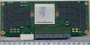
IBM 51Y7638 – Produced Early 2012 – Blue Gene/Q 1.6GHz 18 Core PowerPC-A2

This is a Compute card from an IBM Blue Gene/Q (specifically the 6 rack BG/Q running at England’s Science & Technology Facilities Council Daresbury Lab in Cheshire).  A Blue Gene/Q system is made up of these cards, 32 per ‘Node Card’, and 1024 per rack. This doesn’t count the I/O board which use a similar design and contains 8 Compute cards per rack.
BlueGeneQ ASIC die shot

BlueGeneQ ASIC die shot

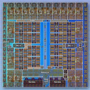
Each of the Compute cards contains a large ASIC (the large chip in the middle).  This ASIC contains 18 PowerPC-A2 processor cores running at 1.6GHz.  16 of them are ‘User’ cores, 1 is for system management (handles interrupts  message passing, etc) and the 18th is a spare, for increased fault tolerance. The ASIC also contains 32MB of shared L2 cache and a dual 1.3GHz memory controller for the 16GB of DDR3 memory on the card.   All said this 45nm chip contains 1.47 Billion transistors, but only dissipates 55Watts, granted, that adds up when you have thousands of them.

A ‘basic’ system contains 4 racks, so 4096 compute cards (4128 if you count the the I/O boards). Together this is 65,536 user cores and consumes upwards of 85kW of power (this actually makes it one of the most efficient super computers available).

So how do these cards become available?  Simply put when you have so many in a system, statistically you are going to have failures, and somewhat frequently.  IBMs target failure rate, based on a 96 rack system (which is massive) is 70 hours.  That’s one failure  every 3 days.  At this point the common reaction is to express shock at the dismal reliability of such a system, however, lets put it another way, that’s one failure out of 98,000+ Compute cards (yes there are other failure points but for the sake of argument we’re using just the compute cards).  If you run an IT department that services nearly 100,000 computers and you only have to fix something twice a week, there is a good chance you should get a raise.
 

Tags:
,

Posted in:
CPU of the Day

February 12th, 2013 ~ by admin

Reading Mask ROMs – With Python image processing

Mask ROM

Mask ROM

Users of the Python programming language often say it can do anything, and that may just be true.  Microcontrollers through out their history have had a variety of ways to store the programs they run.  Unlike a microprocessor, a microcontroller typically has a fixed, or somewhat fixed, program that it runs.  This program is often referred to as firmware (its not software, as its cant easily be changed, and its not hardware as it isn’t discrete chips, thus firmware).

There are several common ways to store firmware:

  • UV-EPROM: The microcontroller has a UV-EPROM as part of its die (or in some cases separate but on the same package).  This can be programmed using higher voltages, and erased/updated, albeit not in the field.  This was popular in the 80’s for prototyping work.
  • Flash (or EEPROM):  This replaced UV-EPROM program storage as it was update-able in circuit, allowing for such things as user BIOS upgrades, updating firmware on CD/Hard Drives etc.  This has become fairly standard for any firmware that is likely to need to be upgraded in the future.
  • Intel B2616 - Unless you clean the paint off

    Intel B2616 – Unless you clean the paint off

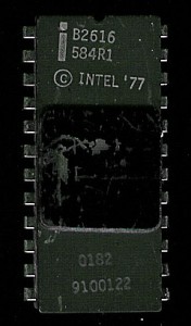
    OTP: One Time Programmable Read Only Memory is useful for medium to large scale production runs.  This allows the code to be ‘burnt’ onto a chip prior to shipping. Often all these were were UV-EPROM chips in a plastic package.  Early Intel’s even used UV-EPROM chips, and simply painted over the window.  a 2708 UV-EPROM became a 2608 PROM with the simple application of some nail polish.  There has been some experimentation and success in erasing/reusing these with the use of X-Rays. (they can penetrate the plastic package).

  • Mask ROM: A Mask ROM is just as it sounds, the program code is actually added to the actual mask itself when making the microcontroller die.  This is the most economical  and reliable for very large production runs.  Obviously one wants to make very sure the code is correct before cutting a mask with it, masks are expensive, and manufacturers are not keen on giving do overs.   In 1978 Intel charged $1000 Mask fee, and a minimum order of 100 units for an 8k ROM (~$10).   By 1986 that Mask fee had risen to $3000 and min units to 1000.

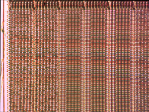
So what happens when 20+ years later you need to figure out whats ON a mask ROM?  The paper tape, 8″ floppy or punch card the program original was stored on is long since gone.  Being that its a mask ROM one can actually SEE the connections, so its possible to decap a device, and visually determine the code, albeit with a lot of tedious work.  Adam Laurie of Aperture Labs developed a Python script to automate some of it, and wrote an article explaining it, which covers some every interesting Mask ROM info.  Not to mention some very nice pictures, so check it out.

Tags:

Posted in:
Just For Fun

February 7th, 2013 ~ by admin

CPU of the Day: Unknown IBM MCM – Any ideas?

IBM MCM

Click for much larger

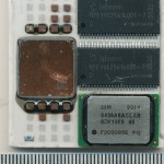
Every now and then I will get a chip in that I cannot ID.  This is a particularly perplexing one.  It looks like it should be something fairly well known, but I cannot determine what.  By the dates its a 2005 vintage IBM, MCM, on a fairly large ceramic package with 1077 lands.  It contains a pair of Infineon HYB39S256160DT-7 256Mbit (4Mbitx16bit) DRAMs which are 7ns 143MHz max, commonly used on PC133 SDRAM.   That works out to 64MB.  Also on the package is a IBM0436A8ACLAB 8Mbit (256Kx36) 4.5ns (222MHz) 1Mbyte SRAM.

IBM MCM die

IBM MCM die

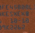
Markings on the die are:
0FE45000L3
AKESXEX0
1 10-10
09K2262


If you have any ideas what it is, or what it may be, post a comment.  I may just give you one.  These came in with a lot of HP PA-RISC processors, so perhaps related?

UPDATE (10/20/2016): Mystery solved. These are processors from a Cadence Palladium emulator system. Read more about them here

Tags:
,

Posted in:
CPU of the Day

February 5th, 2013 ~ by admin

CPU of the Day: The Largest Microchip PIC?

PIC17C766/CL ES

PIC17C766/CL ES

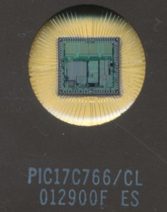
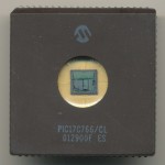
If there is anything a Microchip PIC is known for typically ‘large’ is not what comes to mind.  PICs were originally developed in the 1970s as a peripheral controller and ended up finding uses in products of every sort, for 35 years and counting.  The PIC17 series extended the original 12 bit architecture to 16 bits (16 bit instructions, ALU and registers are still 8-bit).  It added many new instructions (58 total) and an 8×8 hardware multiplier. Max clock speed was 33MHz. It was considered the ‘high end’ of the PIC line but now has been replaced by the PIC18 line.  Most of the PIC17s produced were in the 40-68 pin range. Many designers considered the PIC17 to be a less then great processor and in 2000 Microchip replaced it with the much better PIC18 line.


Microchip PIC17C766-CL-ESThis PIC17C766/CL was one of only 7 variants in the line (17C42,43,44, 752,756,762 and 766) compared to the many dozens in the PIC16 or 18 lines.  Produced in an 84 pin CLCC with UV EPROM window (for its 16k EPROM) the 17C766 provided 66 I/O lines, more then enough for any project.  It was used in some PIC development systems and emulators which were some of the few systems that really needed a PIC with 84 pins.  This particular example also happens to be an Engineering Sample and was produced in mid-2001, AFTER the introduction of the PIC18, it seems there was still at least some demand and use for the PIC17 a decade after its introduction.


Tags:
,

Posted in:
CPU of the Day