September 28th, 2013 ~ by admin

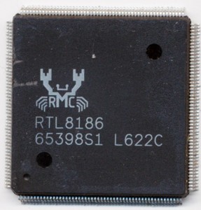
Realtek RTL8186 Lexra LX5280 MIPS with DSP Extensions – 2006
The MIPS architecture was created in 1985 from a project at Stanford University. It was one of the first licenseable architectures. A company could buy a license and make their own MIPS architecture processors. By the 1990’s this had become fairly common and many companies were making MIPS processors, including Performance Semiconductor, IDT, NEC, Toshiba, LSI and more. In 1992 MIPS Computer Systems, Inc. was bought by SGI, in order to guarantee a supply a continued development of new MIPS designs for SGIs computers. It did continue to license the design to other companies as well, fostering competition which helped lower prices for SGI. In 1998 SGI spun off MIPS into its own company once again, as SGI at the time had decided to move towards Intel’s Itanium architecture (this should sound familiar, DEC and the Alpha suffered the same fate). By 2008 MIPS was losing money and in 2013 what little remained (having used most of their cash to buy, and then sell at a loss Chipidea) of them was bought by Imagination Technologies (makers of the PowerVR line of graphic solutions, used notably in the Apple iPhone’s A4, A5, A6, and likely A7 processors). But there is a bit more to the story of MIPS, a seemingly small chapter that very well could have changed history and certainly changed the success of MIPS.
In 1997 a small company called Lexra was started. Lexra was a semiconductor Intellectual Property company. They designed processors and licensed the designs. What made Lexra different is that they designed and licensed soft-cores. A soft core is an RTL (Register Transfer Level) model of the processor. It is usually written and delivered in an HDL (Hardware Descriptive Language) such as Verilog or VHDL and the purchaser may compile it down to whatever actual transistor level hardware they like. This is exactly how ARM works today, but in 1997 ARM only licensed hard cores, cores already compiled down to the gate level and ready for implementation on a given fab process technology. This allowed them to have tighter control over the design and its performance, but made integration much harder into other products. A soft core like Lexra designed enabled rapid integration into a variety of SoCs and other applications. Lexra’s chosen architecture was MIPS and that is where the story gets interesting.
Read More »
September 18th, 2013 ~ by admin
Update: Sept 20th: It has been confirmed that the A7 is still made by Samsung, most likely on their 28nm High-k dielectric process (same as the Exynos in the Galaxy S5). The M7 has also been confirmed to be an off the shelf NXP LPC1800 ARM Cortex-M3, running at up to 180MHz, nothing spectacular, and fairly common for sensor interface. What does this mean for Apple? It means if they can get that much performance out of Samsung’s 28nm process, when and if they Do switch to Intel, the possibilities are quite interesting.
However, its still interesting to play what if, so the below analysis remains.
It has been rumored that Apple’s new A7 processor may be fab’d by Intel, rather then TSMC and Samsung. Previous generations of the Ax have been fab’d by Samsung and in July it was announced that TSMC had picked up an Apple contract. Intel has in the last year begun to market, albeit quietly its excess fab capacity. This is an entirely smart move by Intel. It will help them use their multi-billion dollar fabs to the fullest capacity, as well as test and experiment with other designs.
Apple using Intel as a contract fab makes sense, for Apple. Intel has the best fab technology in the world, bar none. Apple is less concerned with competing on price, than they are making the best devices possible. To have the best devices you need the best (fastest and lowest power) chips. To have the best chips you need the best processes, and that means Intel. None of this is in question. If the A7 is fab’d by Intel it will greatly help Apple attain its market leading position. However, what is in question is whether this is a ‘huge win’ for Intel. One blog even referred to Intel making Apple chips as “That’d be a hell of a score for Intel.” In reality this will have little benefit to Intel. Certainly not financially. Lets look at why.
Read More »
September 15th, 2013 ~ by admin

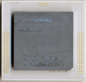
Compaq 21364 Alpha Prototype – 2002
The DEC Alpha was one of the fastest processors of the 1990’s. The original 21064, manufactured in CMOS, rivaled the fastest ECL processors and blew away most everything else. Clock speeds were 150-200MHz (eventually hitting 275MHz) at a time when a standard Intel PC was hitting 66MHz, at the very top end. It was manufactured on a 0.75u process using 1.68 million transistors. The Alpha was a 64-bit RISC design, at a time when 16-bit computing was still rather common. This gave the architecture a good chance at success and a long life.
The 21064 was followed by the 21164 in 1995 with speeds up to 333MHz on a 0.5u process, now using 9.3million transistors. It added an on die secondary cache (called the Scache) of 96KB as well as 8KB instruction and Data caches. These accounted for 7.2 million transistors; the processor core itself was only around 2.1 million, a small increase over the 21064. At the time the main competition was the Pentium Pro, the HP PA8800 and the MIPS R10000. Improved versions were made by both DEC and Samsung, increasing clock speeds to 666MHz by 1998.
In 1996 DEC released the next in the series, the 21264. The 21264 dropped the secondary cache from the die, and implemented it off chip (now called a Bcache). The level 1 caches were increased to 64KB each for instruction and data resulting in a transistor count rise to 15.2 million, 9.2 million of which were for the cache, and the branch prediction tables. Frequency eventually reached 1.33GHz on models fab’d by IBM. However the end of the Alpha had already begun. DEC was purchased by Compaq in 1998, in the midst of the development of the enhanced 21264A. Compaq was an Intel customer, and Intel was developing something special to compete with the Alpha.
Read More »
September 14th, 2013 ~ by admin

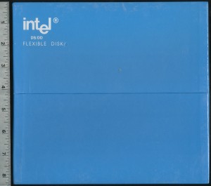
Intel 8″ Floppy Disks (10 Pack) – Minimalist Packaging ahead of its time. 1.2MB
The original floppy disk was introduced by IBM in 1971 as a way to serve updated microcode to their clients mainframes. Each disk could hold around 80KB. By 1977 the DSDD (Double Sided, Double Density) 8 Inch disk was released which held 1.2MB of data. They were officially known as a ‘Flexible Disk’ but floppy disk rapidly became what people referred to them as. Intel marketed and sold them as well as many other manufacturers. Intel accepted code for MaskROM based processors, on 8 inch floppy, tape, and a variety of other formats in the 1970’s. Certainly 1.2MB was a great plenty of storage for the 1-8KB of ROM most microcontrollers and MaskROMs supported in that era.
In 1978 a ‘consumer’ version of the floppy was released, in a more friendly size, but lower capacity. This was the 360KB 5.25″ disk that was eventually made famous by the IBM PC, TRS-80, Apple. and about every other computer of the late 1970’s and early 1980’s. 
Floppy disks continued to evolve into the late 1990’s trying to compete with the CD-ROM, with capacities eventually hitting 240MB with the LS-240 Laser Servo drive. In the early 21st century companies, largely led by Apple, began to delete the floppy from their computer line up, causing quite a stir. However, users quickly realized that contrary to popular belief, the floppy really wasn’t used much. Ultimately the use of the floppy, and the CD have been replaced with the USB Flash Drive, and in many ways, cloud computing.
September 3rd, 2013 ~ by admin

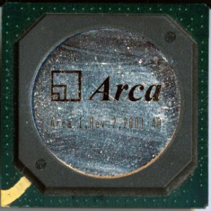
Arca-1 Rev2 166Mhz Processor – Late 2001
China is generally seen as where devices are made or assembled, rather then where they are designed or invented, certainly in the computer world. In 2001 a Chinese Gov’t funded venture known as ARCA Technologies changed that. ARCA (Advanced RISC Computer Architecture) designed and released a completely new processor known as the Arca-1. At the time there were two design houses working to create China’s first CPU. Arca, and BLX. BLX made the Godson series of processors which are MIPS32 and MIPS64 implementations. Arca, took a different approach. Not only did they seek to make an indigenous design, but they wanted to do so with their own Instruction Set Architecture (ISA).
The ArcaISA is, of course, RISC based, it contains 80 instructions, with each instruction consisting of up to 3 operands, and contains 32 general purpose registers. The original Arca-1 design is made on a 0.25 micron process (by which foundry is unclear, BLX used ST) with a 5-stage pipeline and drawing 1.2W at a clock speed of 166MHz. It contained separate 32 way associative 8K caches for Instruction and Data. The Arca also includes a DSP unit that has a pair of multiply/Accumulate Units (MACs) as well as basic SIMD support for media acceleration (including hardware MPEG2). Not exactly impressive for 2001, but not bad for a first release. However there was more to come.
Read More »


