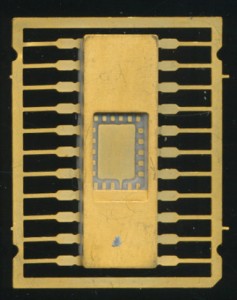
Early Unfinished Ceramic DIP Package
 Most all IC manufacturers do not make their own packaging. Raw packages are purchased form package suppliers such as Kyocera and NGK (among many others). The die is installed, bonded, wired, and tested, and then shipped. This is an early unfinished 22 pin white ceramic DIP. This is typical construction from the 1960’s and 1970’s. The package is supplied as a flat, with the leads straight out and unbent. All the leads are connected by the ‘lead frame’. The lead frame keeps the leads straight during die placement and handling. Only once the die is installed, and the bonding wires connected are the leads (soon to be pins) cut free from the lead frame. The bottom of the die cavity is connected to the ground pin, and the die is affixed to the package with a conductive resin. Typically one of the pads on the top of the die will also be connected to the same ground pin.
After the die is affixed and wired, the device is tested and the leads are bent to form a standard DIP package. In some cases the leads are left unbent and the package becomes a type of surface mount package. A cap is soldered (or s0metimes brazed) over the die cavity, markings applied and then the device is ready to ship.
Tags:
Packages
Posted in:
CPU of the Day

