Chip of the Day: Soviet 573RF10 – a CMOS 8755A
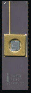
Intel released the i8755 in 1976, the i8755A in 1977 (with better compatibility with the 8085A and 8086/8). The Intel 8755 is an UV- erasable and electrically reprogrammable ROM (UV-EPROM) and I/O chip. The EPROM portion has 16 384 bits, organized as 2048 words by 8 bits. The I/O portion has two general purpose I/O ports, each I/O port is individually programmable as input or output. These were essentially a combination of the 8255 PIO and the 2716 EPROM on a single die/package. These were made on a NMOS process.
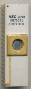
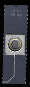
NEC and Toshiba released similar microcircuits behind Intel. Basically, the microcircuit was intended to work together with the 8085A microprocessor. It differs from its predecessor i8080A in that it has a multiplexed data and lower address bus. The standard three-bus architecture of the microprocessor system is obtained by multiplexing with the help of an additional external register. In this register, the low byte of the address is fixed by the special output signal of the microprocessor.
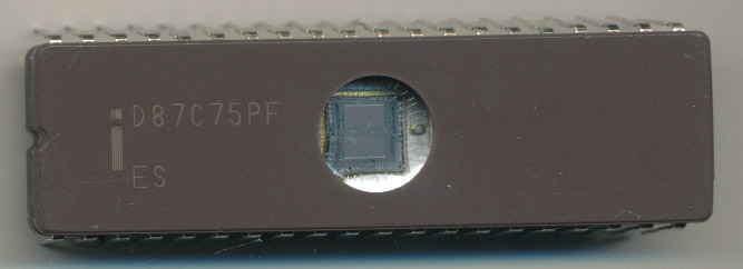
By 1988, the 8755A was obsolete and Intel released the 87C75 instead (see article on the CMOS 87C75).
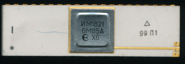
Around this time, the production of an analogue of the i8755A, the 573RF10 microcircuit, began in the Soviet Union. Why start producing a microchip that the world electronics leader is changing to a more advanced one? The fact is that at the beginning of 1988, the production of IM1821VM85A began in the USSR. This was a radiation hard analogue of the CMOS i80C85A. It was with it that the 573RF10 was supposed to work.
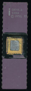
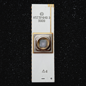
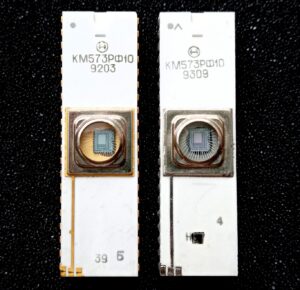
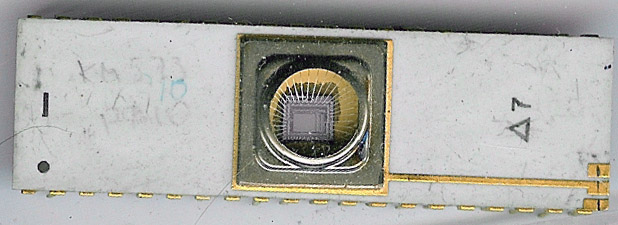
The chip is made in a 40-pin side-brazed ceramic DIP. Supply voltage +5 V. Programming voltage +21 V. It was produced at the Vostok fab in Novosibirsk on a CMOS process (to match the 80C85A).
The 573RF10 is the only CMOS chip in the 573 series.
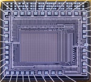 573RF10 die – single memory cell – radiopicture.listbb.ru |
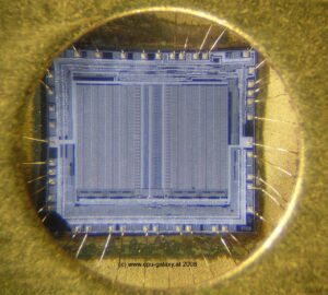 Intel 8755A die – 2 memory cells – cpu-galaxy.at |
It is noticeable to the naked eye that the 573RF10 is own Soviet development. The 573RF10 and i8755A dies are completely different. The i8755 has two memory arrays clearly visible, while the 573RF10 has only one.
It must be said that the application of the 573RF10 chip was not wide enough. And in general, the idea did not take root. The next obvious step in evolution was the combination of a microprocessor, ROM and RAM, input-output ports in one chip which was frequently done on the MCS-48 and MCS-51 series MCU’s which were also being produced in the Soviet Union at the time.
Written by guest author Vladimir Yakovlev
Edited/Formatted by John Culver – The CPU Shack Museum
Pictures – The CPU Shack Museum and others


July 10th, 2022 at 6:31 pm
Were there any improvements made in the 573RF10 ? For example, direct bit set/reset was available in the 8255 PPI but (disappointingly) they left that capability off the 8755 and that was always a 8755 shortcoming for me.
Unfortunately, most vintage hobbyists can’t program the 8755 which is a real shame since it is a very capable chip. The bit programmable DDR was a nice touch, but individual bit/reset would have made the 8755 a killer support chip. Even so, with it’s internal latched address byte, it (and the 8156) is what made the 3-chip MCS-85 possible
July 11th, 2022 at 1:47 am
Verbatim from 573RF10 datasheet :
” Two bit-programmable 8-bit I/O ports (PA and PB)”.
I have a desire to write an article about 1821VM85. Along with it, 1821RU55 and 1821RE55 (analogues of i8155 and i8355) were also produced, which also have I / O ports. I’m going to solder the board so I can test the operation of the RU55 and RF10.