The Oracle SPARC M4 and how it became the M5 (but really didn’t)
The story of the Oracle SPARC M4 is best told starting with Afara websystems. Afara was the original developer of the SPARC processor that became the SUn UtraSPARC T1, aka the Niagara. Sun acquired Afara in 2002 in a sale that was really designed as a capital campaign for Afara, they had the technology and design for the processor, just not the money to enter the market, Sun had the money (or so they thought at the time). The T1 was released in 2005 and had 4-8 cores. The individual cores were called the SPARC S1 core (now an open source SPARC core). In 2007 Sun released the Nigara 2, the UltraSPARC T2, with 4-8 cores, based on the second version of the S1, the S2. Both the S1 and S2 were designed with multi-threading as the primary performance point. They excelled at it, and the UltraSPARC T3, released in September 2010 (though it had been sampling all the way back in Dec. of 2009) did even better at multi-threaded applications. The T3 also was fab’d by TSMC, a change from previous SPARCs which were almost entirely fab’d by Texas Instruments.
The T3, and the S2 core it was based on had one major problem. The S2 core had sub-par single thread performance. While the workloads given to a SPARC server can be tailored somewhat to match was the processor does best (multi-threading) there is always going to be a point at which a single thread task must be done, and it will hold up the entire processor if it cannot be processed efficiently.
The SPARC T4 was designed to fix this. It was based on a new SPARC core called the S3, which allowed much higher clock speeds. The typical T4 has 8 cores and ran at 2850-3000MHz. They had 855 million transistors on a 478mm2 die, using a 28nm process at TSMC. The T4 sampled in March of 2011 and was released in September of 2011, one of the faster times to market for Sun/Oracle. It was packages in a 2386 contact LGA package. (this will become important).
The SPARC T-Series was designed for general high performance computing. It was not designed for enterprise, fault tolerant, or mission critical use. Processors in these environments have all sorts of features meant to deal with hardware and software failures, without bringing down the entire system. Processors and memory can be changed on the fly, and processor types often can even be mixed, with no issue. This is a market that was typically handled by Fujitsu and its SPARC64 VII+ processors. The SPARC VII+ was also known as the M3, being the third generation of the SPARC V used in the M-line of servers. A market Oracle planned to take over, leaving Fujitsu the supercomputer market.
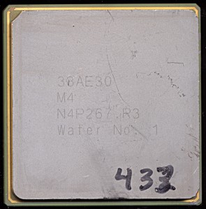
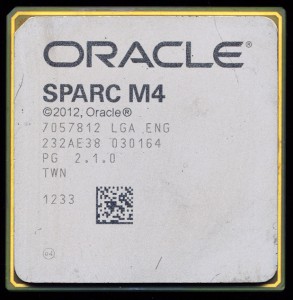
Oracle’s first fault tolerant SPARC was named the M4, because it was to be the successor for the Fujitsu M3. The M4 is a 6 core processor, using the same S3 cores from the T4 SPARC. It has 2 less cores to make room for the additional logic needed for fault tolerance, and upgrades the T4’s L3 cache from 4M to an incredible 48M. The cache alone accounts for 2.3 billion transistors. Like the T4, the M4 was made on a TSMC 40nm process. Die size and transistor counts were never released, but would have came in at around 3 billion transistors. It was packaged similar to the T4, in a 2395 contact LGA package (9 more contacts, but physically the same). The very first samples of the M4 were made in Sept 2011, and testing continued until around Aug. 2012.
The M5 is a rebranded M4…Not likely
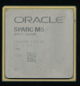
Many sources online refer to the M5 as a renamed M4. The claim is that the M4 was renamed to the M5 to align it with the T5, as they were released at the same time. With that in mind let’s look at the T5. The T5 design began a few months later than the M4 as a follow on to the T4. It uses an enhanced version of the S3 core, and is made on a 28nm process. The process shrink allowed for the cache to be increased to 8M and clock speeds to rose to 3.6GHz and another 8 cores added to the die. The T5 and the M5 were released in March of 2013, fully 6 months after the last samples of the M4 were seen. The M5 samples/development units came out after the last of the M4’s and they are in an entirely different package, using a 2803 contact LGA, 408 more than the M4. The PG revision also started over with the M5. Clearly these are different processors.
The M4 was called the M4 because it was to use the same S3 core as the T4, when Oracle got the process shrink, and the resulting enhanced S3 core, it was used in both the M5 and the T5. The 16 cores and 8M of cache in the T5 take up 511mm2 and use 1.5 billion transistors. The M5, using 6 cores and 48M of cache, uses 3.9 billion transistors in 643mm2.
An M4 sample (PG 1.0.0) die had an area of ~520 mm2, which fits, but only barely. Where does this leave us? The M4 is just that, a S3 cored 40nm M5, The M4 really is an old name for the M5, but in a completely different package (this seems unlikely, unless it needed a lot more power/grounds). Or the third option, the M4 is the announced, but then vanished, 4-core 28nm Yellowstone Falls, designed to support up to 192 sockets.


