TeraNex: Filling the GAPP
The GAPP (Geometric Arithmetic Parallel Processor) was designed in 1981 at Martin Marietta, which later became Lockheed Martin Electronics & Missiles. It was funding in large part by the US Dept. of Defense as a way to develop technologies for ultra high-speed image processing. There was a strong need for image processing, in near real time for military applications, in particular pattern recognition. Being able to process a moving image and match its features to known patterns was very useful for targeting of many weapons system.
The GAPP processor was a massively parallel SIMD (Single Instruction Multiple Data) processor. SIMD works very well on large sets of data that are processed in the same way. In the design of GAPP, this data set was the 2D-array of an image, or frame, from a video. The GAPP is at its core a very large array of simple processors, called processor elements (PE). Each PE is relatively simple, containing a single bit ALU and registers/memory. Each PE handles a single pixel of the image/frame, and is connected in a 2-D mesh to its 4 nearest neighbors. This allows arrays of these PE’s to scale very well. By 1992 Lockheed had GAPP systems with 82,944 elements and by the 2000’s systems were available with nearly 300,000.
In 1998 TeraNex was formed to commercialize this technology, and in 1998 there was a looming problem in television, one that the GAPP, and newly formed TeraNex were well suited to solve.
In the late 1990’s the world of TV was changing, the days of standard def 480p resolutions were moving towards crisper, sharper, more detailed video at 720p and 1080p resolutions. The problem is there was (and still s) a lot of content that TV stations, cable providers and satellite broadcast providers that was in the ‘wrong’ format. This is content that would have to be upscaled, downscaled, or somehow modified to match each broadcasters choice in video standards. There are simple ways to do this (interlacing for example) but these have negative side effects. One of the best ways is to evaluate each and every pixel, based on the pixels around it to convert between resolutions. This means that each and every pixel, a 720×485 frame contains nearly 350,000, needs to be analysed. This is what the GAPP was designed to be able to handle, and what TeraNex did with it.
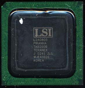
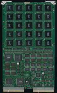
The first TeraNex processors were a 0.35u chip, made by LSI, that contained 1024 PE’s in a 32×32 array. They run at 64MHz (late 0.25u versions ran at 90MHz) and can handle 8-Giga Ops/sec) (GOPS). These were mounted on a card, containing 25 processors, capable of averaging 64 GOPS, and a full, 6-board set could handle a TeraOp.
In 2004 Silicon Optix (now GEO Semi) purchased TeraNex and their GAPP patents, and designed them into even smaller chips. The Silicon Optic Realta HQV processor is a 3072 element TeraNex array controlled, on the same chip, by a 250MHz MIPS processor w/ FPU. These were fab’d by IBM and could handle the same performance of an earlier Teranex 3RU rackmount system costing $60,000, all on a chip that could now be slotted into home entertainment (albeit of the higher end variety) equipment. GEO also has licensed a Realta 2 TeraNex FPGA core that runs at 317MHz with 6144 PE’s (on a 96×64 array), capable of 2 Tera-Op, twice what an entire 6-board TeraNex system could do in the early 2000’s. As video continues to scale, so does the technology to process it, GAPP was designed to scale, and as semiconductor tech continues to improve, GAPP processors become more and more deeply embedded, handling our video conversion needs, without us giving a second thought. Designed for targeting systems on weapons, it now shows us the best explosions entertainment can provide. Lockheed was an incubator of sorts for technology. Intel’s graphics have their roots in another Lockheed venture, Real3D, technology originally designed for tank simulators that became Intel i740 and other embedded graphics solutions.


