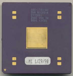
CPU of the Day: Cypress CY7C601 25MHz SPARC
In Mid-1987 Sun Microsystems (now owned by Oracle) released the SPARC (Scalable Processor ARChitecture) processor architecture to be used in their computers (replacing the 68k based systems they had previously used). The SPARC was designed from the outset to be an open architecture, allowing manufactures to license and built processors that implemented it using whatever technology they wished. The goal of this was to 1) build a large SPARC ecosystem and 2) keep prices in check by fostering competition among manufacturers. The SPARC is still used today by Oracle, Fujitsu, the European Space Agency and others, owing largely to its design as an open architecture from the very beginning.
The first version was made by Fujitsu on a 20,000 gate array at 1.2 micron and ran at 16.6MHz. In July 1988 Cypress (later to be spun off as Ross and make the famous HyperSPARC line) announced the CY7C601. This was the fastest implementation of the SPARC at the time. It was made on 0.8u CMOS process and contained 165,000 transistors, dissipating around 3.3Watts. As was typical of many processor designs of the time, it was an integer only processor, requiring a separate chip (the CY7C602) for floating point work. In September of 1988, Cypress cross licensed the ‘601 to Texas Intruments in exchange for rights to the 8847 floating point processor. This was mainly to appease one of Cypress main customers who demanded that a second source for the ‘601 chips be available, a demand more common in the 1970s then in 1988 but Cypress obliged. Cyrpress also gained the rights to make the next generation SPARC processor that TI was developing. TI would go on to make many SPARC processors, and continued to be the primary fab for Sun up through the SPARC T2 Plus in 2008. Oracle now used TSMC to fab the T3 and T4 SPARC processors.


