Archive for the 'Boards and Systems' Category

June 27th, 2021 ~ by admin

Navy Hydrophone Noise Canceller: Weitek 3332 Floating Point Based DSP

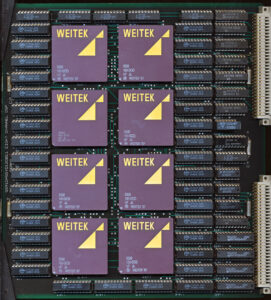
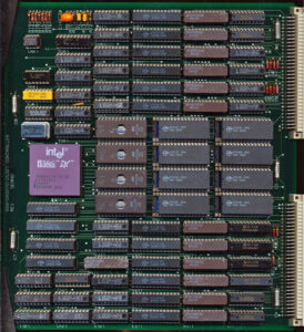
Navy 55910 ASSY 0120811 Eight Channel DSP – Serial #1

I got these boards some time ago, hoping to be able to figure out more about them but alas, information is very sparse, but they are such good looing boards, with impressive technology for the day, I had to post them

These boards came out of a US Navy system labeled “Hydrophone Noise Canceller”  which seemed to be part of SONAR test system at a University.  These date from the late 1980’s to the early 1990’s. The system was comprised of 16 boards, 12 8 Channel DSP board, a control board, and 3 Ethernet Boards,  Each of these boards is a very heavy 4 layer PCB, with pretty much everything socketed.

The DSP Boards are based on the Weitek 3332 FPU. These are full 32-bit Floating point datapaths (MULT/DIV/ADD/SUB + Registers) and made on a CMOS process.  They operate on a 100ns (10MHz) clock.  THese are the higher end version of the 3132, they have a full 3 busses versus the single bus of the 3132.  These 3 busses add a lot to the pincount (168 vs 144) and thus cost but make designing a system more flexible, no bus sharing to worry about.  The 3332 was designed specifically to support high speed DSP and graphics processing.  It performed the ‘core’ of a DSP, allowing the user to build around it and make essentially a custom DSP for their application (unlike the purpose built TI TMS320 series of DSPs also available at them time) On the board they are backed by 4 Cypress CY7C128 2K SRAM per processor (8K total).  There is no clock crystal on the board itself, which is typical of a system like this.  To ensure everything stays in synch, the clock would be provided by the control board and distributed to each of the boards on the bus.

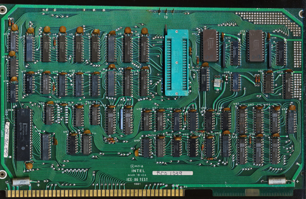
Navy 55910 ASSY 0125321 Controller A80386DX-25 (20MHz) Serial #2

The Control Board runs an Intel A80386DX processor.  On this particular board its a 25MHz chip, but note the crystal next to it is an 80MHz crystal.  A 386 internally divides the clock by 2, so the 80MHz clock is most like divided by 2 externally resulting in a 40MHz input to the 80386, and a 20MHz CPU clock.  I had another controller board with a 20MHz 80386 so they probably just used what ever they had available.  This is Serial # 2 afterall.  The 386 is supported by 4 27C256 EPROMs and 8 32K (CY7C198) SRAM chips, giving it 256K of SRAM.  In addition is 12 8k (CY7C185) 8K SRAM chips each with there own Pipeline Register.

A typical 386 system would have several MB of RAM, but this system is set up for real time data processing, as a DSP system, so the only data that needs to be in RAM is the control program itself, so 256K of system RAM is a great plenty.  Additional RAM is likely used solely for buffering data from the Hydrophones.

It would be interesting to know what this board was used for in more detail, but even if that never happens its an interesting board for its time.  Clearly a vast amount of effort went into designing and building the system.


Tags:
,

Posted in:
Boards and Systems
May 17th, 2021 ~ by admin

First & Last AMD Socket A Athlons – Thunderbird vs. Barton – Part 2

Continuing our exploration of the evolution of the Socket A architecture.  See Part 1 here

Test Stand

For tests of all processors with a final frequency of 1 GHz, several processor / RAM operating modes were selected: 100/100, 100/133, 133/133, 133/166 MHz, priority was given to modes with the highest RAM frequency.

The main components of the system:

CPUs:

AMD Athlon XP-М, (10x 100 и 7.5x 133) 1000 MHz, Barton
AMD Athlon (B), (10x 100) 1000 MHz, Thunderbird
AMD Athlon (C), (7.5x 133) 1000 MHz, Thunderbird

Motherboards:

  • ASUS A7V, chipset VIA Apollo KT133
  • ABIT KR7A, chipset VIA KT266A
  • EPOX EP-8K3A, chipset VIA KT333
  • EPOX EP-8K9A7I, chipset VIA KT400A
  • EPOX EP-8RDA3I, chipset Nvidia NForce 2 Ultra 400

Memory:

  • OCZ PC3200 EL Platinum Edition (OCZ4001024ELDCPE-K), 512 Мб х2 (PC3200) CL=2

Videocard

  • Gainward – GeForce 6800 Ultra AGP 256 Mb (Forceware 81.85).

Testing was carried out in Windows XP Sp3 using the following software:
• Super Pi mod. 1.5XS (1M task)
• PiFast v.4.1
• WinRAR x86 v. 5.40
• Cinebench 2003
• 3Dmark2001SE Pro b330
• 3DMark 2003 v.3.6.1
• AIDA64 5.50.3600
• PCMark 2004 v.1.30
• Max Payne
• Far Cry
• DOOM III

Tests

When testing all platforms, I used the same Windows XP SP3 distribution with the same list of running services and settings. Gainward GeForce 6800 Ultra AGP 256 MB together with Kingston V300 60 GB SSD remained unchanged companions throughout the tests. Windows XP SP3 was installed from scratch for each platform. All VIA chipsets used VIA Hyperion 4-in-1 Driver version 4.51. For the video card – Forceware 81.85. All unnecessary services were disabled, the system was tuned to high performance mode.

Read More »

Posted in:
Boards and Systems

May 14th, 2021 ~ by admin

First & Last AMD Socket A Athlons – Thunderbird vs. Barton – Part 1

Introduction

The AMD Socket 462 or Socket A, was a rather interesting and long-lasting CPU Socket. The first models of Socket 462 processors appeared in the summer of 2000, they were just the first representatives of the AMD Athlon “Thunderbird” in a ceramic case with a clock frequency of 600 MHz, and with 256 KB of L2 cache , an effective system bus frequency of 200 MHz, with MMX support instructions and their own 3DNow !, of course, there was no question of any SSE in those days. Produced ” Thunderbirds” at 180 nm. tech process, the operating voltage was set in the range of 1.70-1.75 volts, and the maximum heat dissipation was 72 watts for the older model 1400 MHz versions.  These replaced the old Slot A cartridge based Thunderbirds, made possible by the L2 cache being moved on die instead of off die (in similar fashion to Intel’s Coppermine Pentium IIIs moving to S370 from Slot 1).

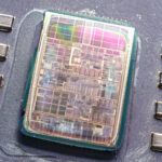
Thunderbird die exposed

The last representative that was designed for Socket 462 was AMD Athlon XP+ using the “Barton” core, released in early 2003, which retained its position throughout 2004. With “Barton” the ceramic case is a thing of the past, being replaced by a Organic PGA package. The process has decreased to 130 nm, the L2 cache capacity has doubled, the system bus frequency has doubled, and the clock speeds have exceeded 2.2 GHz.

The fastest model had a real frequency of 2200 MHz and a performance rating of 3200+, the operating voltage was 1.65 V, and the TDP was 77 W with a 400FSB.  These was also another AXDA3200 with a 333 FSB, this actually clocked slightly faster as 2.333GHz, but was given the same PR rating due to its slightly slower FSB. The processor acquired the first generation SSE instructions, and the motherboards created for it in that day now added support for dual-channel operation of the RAM. If we add here that the first motherboards based on Socket 462 worked with SDRAM memory, and the subsequent ones with DDR-SDRAM, then according to a number of indicators there is a twofold increase in the main characteristics of the platform within the framework of one socket.

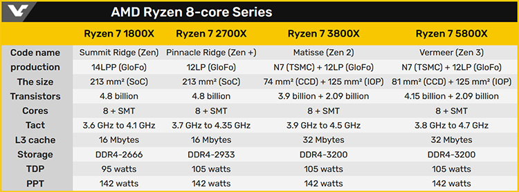
Such a funny comparison reminded me of today, where from the time the first generation of AMD Ryzen processors appeared in 2017, until the last (fourth gen), which debuted at the very end of last year (2020), all processors also had one AM4 socket. Ryzen performance gains across all four generations are clearly exemplified by the following slides:

AMD hasn’t had much of a problem with processor support before, although AMD has officially announced that Ryzen 5000 series desktop will only be supported on boards with 400 and 500 series chipsets. Therefore, on motherboards released for the first generation Ryzen, it will not work to use the latest generation processors in an official way. Although there is information on the network that there are cases of using Ryzen 5000 series processors on motherboards with the older X370 chipset, but the official position of AMD has already been announced above.

In the wake of such analogies, I thought, why not compare the first and the last Athlons for Socket 462 on several motherboards at the same clock frequency, with the same system configuration? You will find out the result of what came out of this by reading this article to the end.

Continuation of the Idea

The essence of the idea is simple – take the first AMD Athlon based on the “Thunderbird” core with a 200 and 266 MHz system bus and a clock speed of 1 GHz and an AMD Athlon XP representative on the “Barton” core with a similar round frequency of one GHz, and compare them with each other to find out how much the first generation loses to the last one. During the existence of Socket 462, several generations of processors with different cores have changed on it: Thunderbird – Palomino – Thoroughbred – Thorton – Barton.  This will be an interesting test of raw architecture improvements of the core. all other things being as equal as they can be.

Read More »

Posted in:
Boards and Systems

February 25th, 2021 ~ by admin

The 486 CPU Era – The Birth of Overclocking. – Part 2

In Part 1 of The 486 CPU Era – The Birth of Overclocking, we covered some of the basics of the 486 era and where it came from, as well as the various brands/types of 486s of the era (many of which we will test and attempt to overclock.  In Part 2 we will discuss the hardware selection and rational, testing environment and benchmarks! (and a healthy dose of Overclocking with some perhaps surprising results)

Choosing a Motherboard

Socket 5, GIGABYTE GA586AM, UM8891BF / UM8892BF chipset – Good but not good enough

Choosing a motherboard for the 80486 platform is not easy. There are several criteria or approaches for the implementation of such projects. 1. Consider whether you need PCI slots? 2. The need for VLB slot(s) 3. The need for everything on one board.

Since I set myself the task of assembling the most productive Socket 3 system, the presence of ISA and VLB slots was a secondary matter for me, PCI slots were a priority due to their speed characteristics. The fastest chipset was required from the motherboard – this is the UMC 8886/8881. Revisions of this chipset were later used in Socket 5 Pentium motherboards that supported FSB 60/66 MHz and higher. The board must have 4 slots for RAM with support for EDO RAM, the minimum total size is 128 MB (4x 32 MB).

The total size of the L2 cache should be equal to 1 MB, so the motherboard should contain 8 sockets for such microcircuits.

Due to the use of different processors with different input voltages, the board must support a choice of voltages from 3.3 V to 5 V in small steps, in order to be able to “smooth” overclocking. Accordingly, the overclocking capability on the bus from 33 to 50 MHz and higher should be implemented. So which board do we end up with?

Read More »

Posted in:
Boards and Systems

February 21st, 2021 ~ by admin

The 486 CPU Era – The Birth of Overclocking. – Part 1

Introduction

486 CPU Era – the birth of Overclocking – this is how I decided to call everything that was in the pre-Pentium era, which I did not find and become familiar with until a couple of months ago.

(Another Article in cooperation with max1024 of Belarus – Edited/Expanded by Me)

If we abstract from the very first Pentiums, which appeared using Socket 4 in two speeds of 60 and 66 MHz, then these processors won popular fame and love in motherboards based on Socket 5 and 7. Such machines could be seen in the early 90s on which while playing C&C, Warcraft and other RTS games. The Sega Mega Drive II and Super Nintendo game consoles competed with expensive computers. Moreover, the consoles were far ahead in popularity (and to be honest, the graphics and game play were better) and I got used to the joystick much earlier than to the mouse and keyboard.

The question arises, what was there before all these Pentiums? And the answer, if you dig deeper, can discourage or even confuse any inveterate computer enthusiast, since the cultural layer of “hardware” from the very first processor belonging to the x86 architecture to the first representatives of the superscalar architecture is much larger than from the Pentium 4 to the freshly released Intel Core i9-11900K, which belongs to the Rocket Lake family of 11th generation Intel Core processors. It is not so easy to digest this entire historical layer, so I have outlined the framework for myself.

To simplify the chosen concept, I decided that the platform should in any case support the PCI interface, since it is, firstly, relatively fashionable and “modern” and, secondly, gives more room for my experiments with the accumulated PCI expansion cards. I did not impose other, special requirements on the test platform, except that according to the established tradition, it should be the most powerful and fastest set that is possible to assemble.

Here I think some of the readers of this article the “True oldies” will say: “what is this nonsense, where is the ISA, VLB and 8-bit only?”, But everything has its time, we will gradually dive into the depths of the prehistoric hardware sea, otherwise decompression cannot be avoided. [Editor’s note, I grew up on an 8-bit 8088 and of course connected the PC Speaker to a 100 Watt Stereo Amp, the loudest 8-bit beeps ever]

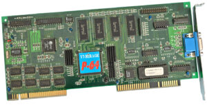
typical VLB videocard – V7 Mirage P64 on S3 Vision 864, 2 Mb (before they hid all the good stuff with a heatsink)

So, let’s play from the presence of the PCI bus, which appeared just during the heyday of 4th generation processors, “fours” or simply – four hundred and eighty-sixths, which first appeared back in 1989 or today it is 32 years ago. “Almost like yesterday” the oldies will say, “We were not born yet,” the rest will answer, although this is not the point.

The previous generation of 386 processors was content to exchange data with peripheral devices more often at the “width” of 8 and 16 bits, although the entire generation of processors belongs to the first microprocessor architecture supporting 32 bits, but despite this, motherboards designed for them had no  32-bit PCI bus. Although this could not have happened historically, since the specification is new, in relation to the previous buses, it (PCI) was first implemented in 1992. This means that the whole choice comes down to the whole variety of 486 processors, and there was enough variety in those years, not that today there is a choice between “red” and “blue”.

Read More »

Posted in:
Boards and Systems
September 29th, 2020 ~ by admin

Aircraft Instrumentation, Bitchin’ Betty and an 80C86 CPU

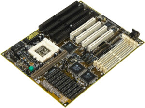
F-15 with P4 Instrumentation Pod – Looks like a missile under the wing, with blue and red stripe.

Quite the combination I know, but of course all related.  Last week I got some boards in that were quite interesting.  They were all fairly early serial numbered, from the 1980s and military in design.  Now one thing about anything military is identifying it is pretty hard to do, especially when it hails from an era before the Internet.  Many records from the 1980s have made it online, but OCR and transcription errors abound, a single wrong digit can turn an item made for a A-4 Skyhawk into a new blade from a lawnmower or a shiny new Navy mess tray.

Thankfully these boards all had a CAGE code which the US uses to identify each and every supplier.  In this case that code was 94987 which is Cubic Defense.  Cubic didn’t make lawnmower blades or mess trays but they did make a lot of instrumentation systems for aircraft (and they continue to do so).

F-16 with blue training pod under its left wing)

It turns out that training fighter pilots is best done without having to use live weapons, for obvious reasons, but in all other aspects should remain as true to lifer as possible, and then be able to be analyzed after that fact in order to learn from mistakes, and see who gets bragging rights for pulling the most G’s.  This means that the aircraft has to send and receive data as it would in combat, threat warnings have to go off when targeted, missiles have to be ‘launched (while being captive) at the appropriate times, and every aspect of the flight must be recorded, speed, roll rates, altitude, etc.

Cubic made pods, that attached to one of a fighters weapon hardpoints (typically the outermost) that did exactly that.  These pods interface with the aircraft’s flight systems (using the standard 1553 bus) as well as with ground based systems on the training range, forming a complete picture of what is going on between all the aircraft taking part.  These particular boards are from Cubic’s second generation digital pods, the P4 series (the first gen was, the P3). Specifically the P4A series.  Each pod contained a vast amount of sensors, antennas and instrumentation to monitor and record what was happening, as well determine if a missile as ‘launched’ to or from the fighter.

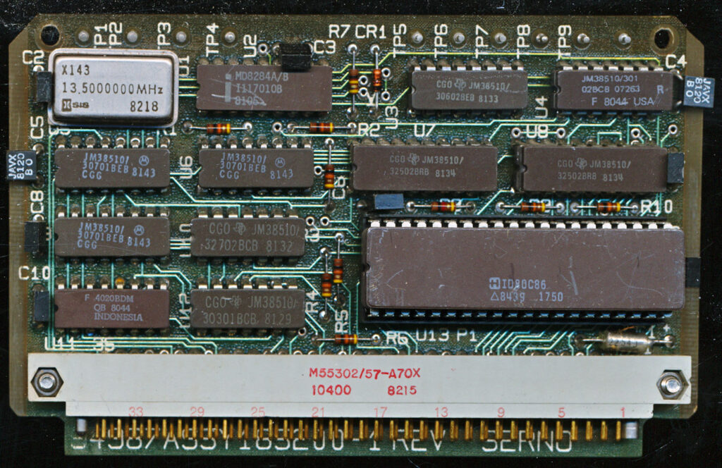
Cubic 185200-1 with Harris ID80C86 – The brains of the AN/ASQ-T25 P4AM Training Pod

At their heart was a Harris or Intel 80C86 processor, (Harris actually did the CMOS conversion on the 8086).  This is one of the earliest applications of the CMOS 8086.  In this case the 80C86 is running off of the normal 8284A clock generator and a 13.5MHz crystal. This results in a processor frequency of 4.5MHz, a bit under its 5MHz rating.  This is pretty typical of military applications, it generates less heat, draws less power, and gives more margins.  This particular board has a industrial spec CPU, later production versions had a full military qualified part (this board was a prototype).

Read More »

September 9th, 2020 ~ by admin

Finding the Limits of the Socket 8

Socket 8 processors have something magical and I really enjoy working with them. Earlier I wrote about them more than once and it would seem that everything has already been said, but in this article you will find out which PC configuration is truly the fastest on Socket 8, although it never existed in reality. I just gave this platform what it never had, it’s like giving the first representatives of the Skylake processor architecture, which was released back in 2015, DDR5 and PCI-Express 4.0 today.

Before starting another fascinating story about Socket 8 and the processors that were installed there, I will give links to my previous experiments:

Chapter 2: Mini-Mainframe at Home: The Story of a 6-CPU Server from 1997
and what got us started…
Part 1: Mini-Mainframe at Home: The Story of a 6-CPU Server from 1997

As you can see, my close acquaintance with this socket has existed for a long time and over the past few years we have clearly managed to make friends. It would seem that all Socket 8 processors have been studied and tested in various configurations, including an insane configuration of six processors in such a monster as the ALR Revolution 6×6. But quite recently I got my hands on a motherboard made by ASUS, which gave me the opportunity to take a fresh look at the use of processors and the performance they are able to give in a newer platform.

What is this board and what chipset is it based on? To name the heroine of today’s article, I will first dwell on the main chipsets for Socket 8 processors. The first chipsets for Intel Pentium Pro processors appeared in November of 1995, 25 years ago. Already at that time, they understood that the future was behind the parallel execution of various tasks. The Intel 450KX chipset, codenamed “Mars”, was introduced for workstations, and the Intel 450GX “Orion” for servers. Mars allowed for dual-processor configurations, and the Orion officially supported up to four physical processors. Although on the example of the super-server ALR Revolution 6×6, which is based on Intel 450GX, the number of processors could have been much larger and could easily double the official figure.

Nowadays the term chipset is often associated with a single chip located on the motherboard, but when applied to the first chipsets for Intel Pentium Pro processors, we are dealing with the physical seven chips that made up the “number of special chips” or “chipset.” These chipsets supported slow FPM DRAM standard RAM, the server GX chipset could operate with 4 GB of such memory, while the KX “was content” with 1 GB support (Intel figuring a workstations needed less RAM then a server). By the standards of the second half of the 90s, these were immense volumes of RAM

In May 1996, a more progressive chipset appeared – Intel 440FX “Natoma”, which quickly began to replace older system logic sets. Intel 440FX itself already consisted of a pair of microcircuits, support for SMP, faster EDO / BEDO DRAM memory types along with the outdated FPM DRAM (though limited to 1GB max of RAM), a new version (2.1) of the PCI bus standard, as well as support for Intel Pentium-II processors were announced.

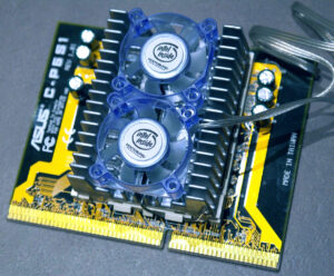
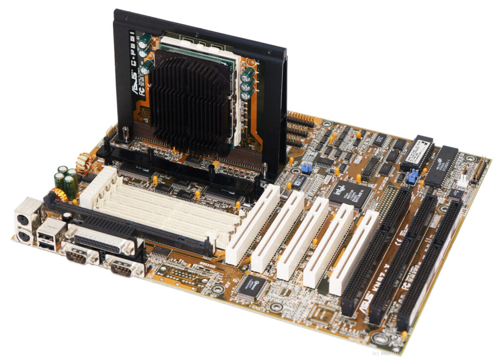
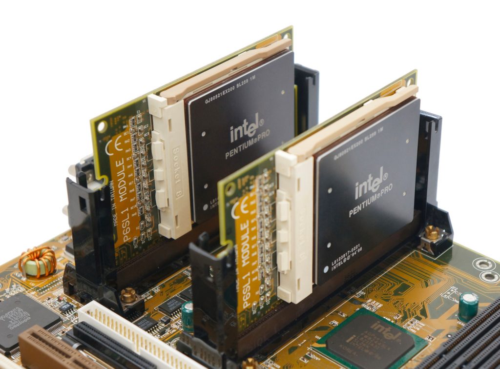
Most motherboards based on the Intel 440FX “Natoma” chipset have a physical design in the form of a Socket, where the processor was installed, but there were exceptions with a few using the new Slot 1 slot, where the first Pentium-II and Pentium Pro were installed through special slot adapters. A good example is the ASUS KN97-X motherboard with the included Socket 8->Slot 1 adapter called the ASUS C-P6S1.

ASUS KN97-X motherboard with ASUS C-P6S1 slocket adapter

Each manufacturer of such slot motherboards produced their own slot adapters, but due to their small circulation, finding them is now problematic. Socket 8 processors feel good in such adapters and the presence of a more modern infrastructure of such motherboards obviously contributes to an increase in performance. But Intel, having released the Intel 440FX chipset, decided to stop further support for its Socket 8 processors, although it could really have extended their life cycle.  Why just sell people a new motherboard chipset, when you cold ALSO force them to buy a new CPU to go in it?

Read More »

Posted in:
Boards and Systems
May 13th, 2020 ~ by admin

Chapter 2: Mini-Mainframe at Home: The Story of a 6-CPU Server from 1997

At the end of 2018, I started one project, which was called “Mini-Mainframe at Home: The Story of a 6-CPU Server from 1997”. It was dedicated to the ALR Revolution 6×6 super server with six Intel Pentium Pro processors and a cost comparable to that of a brand new Ferrari in 1997. It took some 450 days and finally follows the continuation of the story, the super server received the long-awaited upgrade – six Intel Pentium II Overdrive 333 MHz Processors! For those years, such power was simply colossal, but how it compares with today’s and how much increased performance you will learn from this article.

I’ll admit 450 days is quite a long time, so I will briefly recall the contents of the previous series of the article.
And it all started like this: plunging into the world of mainframes and supercomputers , I wanted to try some super powerful system and the choice fell on the ALR Revolution 6×6 super server, which had six Socket 8 and supported up to 4 GB of RAM. For the late 90s, these were scary numbers, as well as its cost. One processor for such a system was estimated by Intel at $ 2675, and six were required, for one module of 256 MB of server memory it was necessary to pay $ 3500, and sixteen sticks were needed to get the coveted 4 GB of RAM.

A disk subsystem was also available with seven raid controllers and an 860 GB disk array, a twenty-kilogram power supply unit and the server itself … As a result, it was possible to reach amounts from 270 to 500 thousand dollars, and if you add here the inflation level over the years, these numbers will range from 435 to almost 800 thousand dollars. Now, in terms of performance, any low-cost computer will be faster than this monster, but the very fact of having such an opportunity in 2020, to feel the full power of that time, makes these large numbers insignificant, it is much more important to find and assemble such a monster.

ALR 6×6 Available Options

In the previous story, I studied performance with six Intel Pentium Pro processors with a frequency of 200 MHz and a 256 KB second-level cache and even overclocked all six copies to 240 MHz. As well as six top-end Intel Pentium Pro “black color” with a frequency of 200 MHz and a 1M L2 cache, which were able to overclock to 233 MHz. In my configuration, I had 2 GB of RAM standard FPM, 16 memory modules of 128 MB, which took over 4 minutes to initialize during the initial POST procedure.

Four gigabytes of RAM would bring this figure to 9 minutes, which is comparable to accelerating a train or taking off an airplane, although the latter can do it much faster. But then, having loaded at my disposal, six physical cores arrived at once, but without the support of MMX and especially SSE instructions.

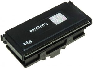
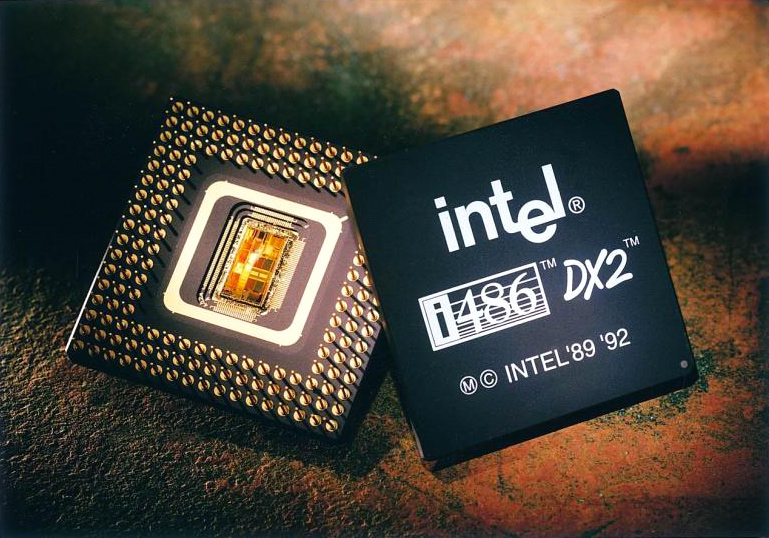
Intel Pentium II Overdrive 333 MHz processor

The basis of any computer is the central processor. Intel Pentium Pro processors first appeared in 1995. Then there were the usual Pentiums without the Pro prefix, but this prefix in the name of the models said that these processors are positioned primarily as solutions for servers and workstations with their special Socket 8. The usual Intel Pentiums were installed in Socket 5 and 7. A significant difference between the Pro and the regular version of the Pentium desktop was the presence of a second-level cache in the Pro version, which, being on the same package, worked at the processor’s core frequency, thus allowing it to significantly increase performance.

For the various Intel Pentium Pro models, the L2 cache size ranged from 256 KB to 1 MB. Pentium Pro’s first level cache was 16 KB, of which 8 KB was for data and the same for instructions. For the subsequent Intel Pentium-IIs, the second-level cache worked at half the processor core frequency and amounted to 512 KB for all models, and it was located in the form of separate microcircuits on the cartridge at a distance from the CPU die itself. The L1 cache size was doubled in size to 32K, which offset the performance hit of the slower L2 cache.

Pentium Pro Slot 1 Slockets – Also made were Slot 2 versions.

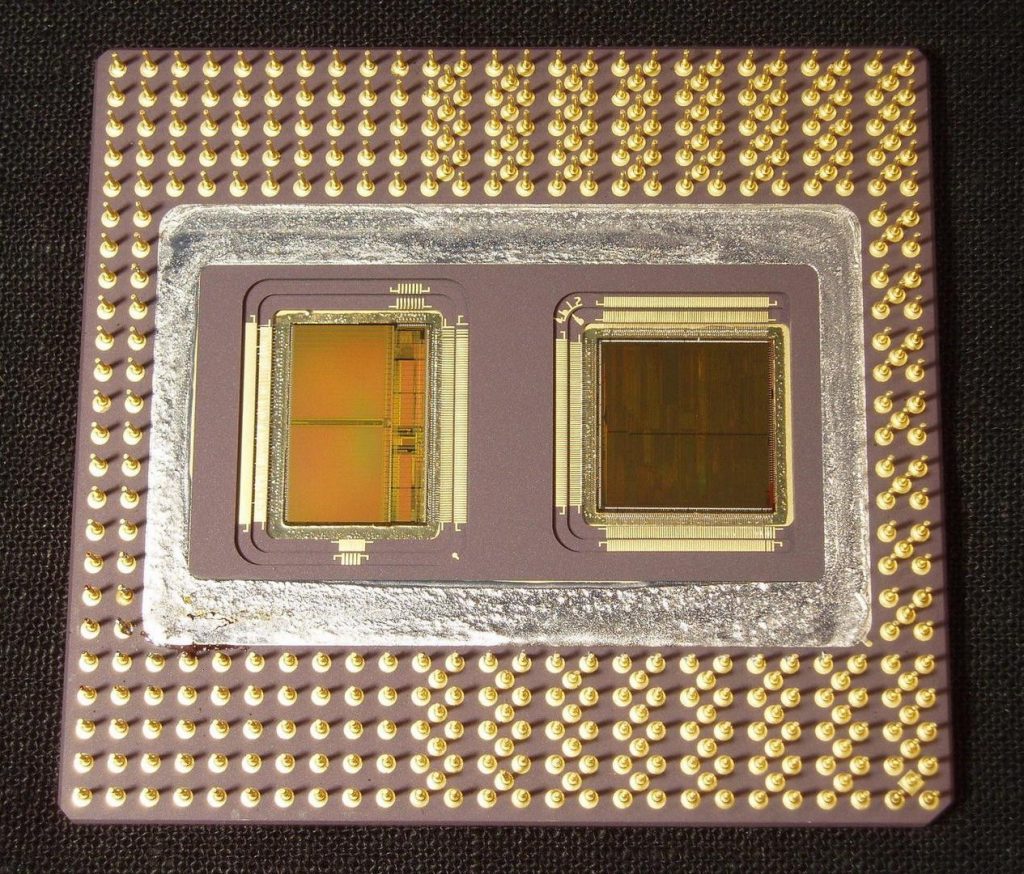
The tested processors were produced at a 350 nm process technology. The number of transistors in the Pentium Pro totaled 5.5 million for the processor core itself and as many as 15.5 – 31 million were in the L2 cache memory, depending on its size. The L2 cache itself was located on a separate die near the CPU core. The processor had a free multiplier and the system bus frequency, depending on the model, was 60 or 66 MHz. Overclocking of the processor rested on overclocking the L2 cache, it the limiting factor.

CPU core on the right, L2 cache on the left

The Intel Pentium II Overdrive 333 MHz was a very interesting processor. This processor appeared, it can be said, thanks to the US Government, which funded a program to create supercomputers for modeling nuclear explosions and tracking the state of the country’s nuclear arsenal. The US government allocated funds for the construction of such a supercomputer, Intel won the tender and in 1997 handed over a turnkey supercomputer called “ASCI Red”.

Read More »

Posted in:
Boards and Systems

October 1st, 2019 ~ by admin

The Story of the IBM Pentium 4 64-bit CPU

Introduction

This time we will talk about one unique Intel processor, which did not appear on the retail market and whose reviews you will not find on the Internet. This processor was produced purely by special order for one well-known manufacturer of computer equipment. Also in the framework of this article I will try to assemble one of the most powerful retro-systems with this processor.
From the title of the article, I think many people understand that we will talk about the Socket 478 Intel processor

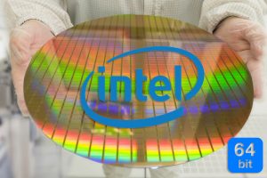
Most people are familiar with the Socket 478 that replaced Socket 370 at the end of 2001 (we omit Socket 423 due to its short lifespan of less then a year) and allowed the use of single-core, and then with Hyper Threading technology “pseudo-dual” processors that can perform two tasks in parallel. All production Intel processors within Socket 478 were 32-bit, even a couple of representatives from the Pentium Extreme Edition server segment on the «Gallatin» core. But as always there are exceptions. And this exception, or to be more precise, two exceptions, were two models of Pentium 4 processors with the Prescott core, which had 64-bit instructions (EM64T) at their disposal.

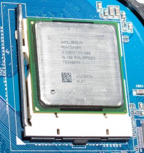
Intel Pentium 4 SL7QB 3.2GHz: 64-bits on S478

This pair of processors were commissioned by IBM for its eServer xSeries servers. These processors never hit the retail market and their circulation was not very large, so finding them now is very problematic. It is interesting that the fact that if you want and naturally have the right amount of money, or a large enough order, you can count on a special order of the processor that is needed for the specific needs, with characteristics that will be unique and will not be repeated in standard production products. And it should be noted that not a few such processors have been released, in fact, in the 70’s and early 80’s this was the very purpose of the now ubiquitous ‘sspec.’ Chips with an Sspec (Specification #) were chips that had some specification DIFFERENT from the standard part/datasheet.  A chip WITHOUT a sspec was a standard product.  By the late 1980’s all chips began to receive sspecs as a means of tracking things like revisions, steppings, etc.  I will talk about some a little later.

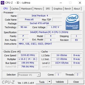
hat’s how the processor looks through the eyes of the CPU-Z utility. In the “Instructions” field after SSE3, the EM64T proudly shows off! Link to popular CPU-Z Validation.

Special processors made for IBM belonged to the Prescott core and were based on E0 stepping with support for 64-bit instructions, which is not typical for Socket 478! The first 64-bit CPUs for “everyone” appeared only with the arrival of the next LGA775 socket, and even then it wasn’t right away; some Pentium 4 models in LGA775 version were 32-bit. I specifically pointed out that the Pentium 4 Socket 478 model with EM64T support belonged to the E0-stepping, although later the more advanced stepping G1 was released, which did not have such innovations. The first model worked at a frequency of 3.2 GHz and had a SPEC code – SL7QB, the second was slightly faster with a frequency of 3.4 GHz and the SPEC code – SL7Q8.

For the rest, these were the usual «Prescott». But the presence of 64-bit instructions made these processors unique, capable of working with 64-bit operating systems and the same applications, allowing them to do what their 32-bit comrades simply could not do.
Read More »

August 14th, 2019 ~ by admin

How to 386 Your AT: Intel Inboard 386/AT

With the release of the 32-bit Intel 386 processor in 1986, owners of IBM PC/XT and AT type systems (8088 and 80286 systems) were left a bit in the dust.  This was a concern (or opportunity) for Intel as well. They designed an upgrade solution at the same time as the 386, to be able to be used in the now obsolete computers.  This was the Intel InBoard 386 series of upgrade cards.
InBoard 386 AT with 1MB of RAM and 80287 FPU Option (very unusualy on a late model Inboard, this one from 1990, but the FPU is from 1986)

The InBoard, as its name implies, was a internal 16-bit ISA card that was used to upgrade these systems.  It included a 386DX processor running at 16MHz, 64K of cache, and (optionally) 1-3MB of additional RAM.  Two version of the board were made: the PC/XT version was designed for 8088 processor based systems, and the AT version was for the 286 systems.  These boards required the removal of the original processor, and then a cable was ran from the old CPU socket, to the the InBoard 386 board.  On system start up the original BIOS booted the system, and loaded the DOS operating system.  The config.sys file would then call on the drivers to load the InBoard 386 specific features.  The original system was essentially unaware of the new processor, instructions were executed by the InBoard transparently.

Flat Ribbon Cable used for connecting the board to the old CPU socket. If the cable could not reach the socket, your system was not compatible. Cable length was restricted by signal timing, rather then the common complaint of Intel being ‘stingy’

Early AT systems used a 6MHz CPU and ISA bus speed, so Intel provided a 8MHz crystal to replace the original on the motherboard. This ensured the ISA bus that the InBoard used to communicate with the original memory and peripherals ran fast enough and did not become such a huge bottle neck.   The base model InBoard did not come with any RAM, it could use your existing system RAM just fine.  Adding RAM, however, was a worthwhile upgrade.  The Board itself supports 1M (36 100ns 256 kbit chips, including parity) and a daughter card could add another 1M or 2M.  This RAM was accessed via the 80386s 32-bit address bus so was much quicker.  It also was a single wait state access.  You could configure the InBoard to backfill (take over for) your existing system RAM, at least down to 256K, so that the computer would only use the first 256K of the slower RAM before moving to the RAM on the InBoard.  If your system had 512K of RAM you would ‘waste’ half of it but at the benefit of much faster access times.  The Inboard 386 had another trick up its sleeve to improve speed…
Read More »

Posted in:
Boards and Systems