Archive for the 'CPU of the Day' Category

May 3rd, 2015 ~ by admin

AMD AM29501: 8-bits to the ByteSlice

AMD AM29501DC - 10MHz Byte Slice

AMD AM29501DC – 10MHz Byte Slice

AMD is well known for its 2901 bit-slice processor of the 1970’s (being made well into the 1990’s), as well as the previously detailed AM29116 16-bit processor released in 1981. However, the 1980’s brought another AMD design as well, though not as complicated, it is no less interesting.  In 1981, there was not a clear DSP (Digital Signal Processor) architecture, or really purpose built design.  The Signetics 8X300 was well suited for such work, but was not inherently designed for it.  DSP tasks were handled by other processors, or by completely custom designs.  The AM29501 was not designed as a DSP, but it was marketed as a signal processor, at least for the first 5 years of manufacture.  What the 29501 was, was a relatively fast, and pipelined, byte slice processor, basically a highly upgraded AM2901.

As the name suggests, the 29501 processes data 8-bits at a time, and as a slicer, it requires external program control (it lacks a PC (Program Counter) or sequencer).  It has an 8-function ALU, and 6 sets of registers, which can be accessed independently, allowing for a pipelined architecture, multiple instructions may be issued before the first one is completed (as long as they don’t need the same resources).  While the ALU is doing some addition, more data may be fetched, or output to one of the 3 8-bit buses. AMD designed the 29501 to be able to do advanced DSP work, and such work requires multiplication, which is something the ‘501 cannot do itself.  The 29501, however, was explicitly designed to interface to the AM29516/7 16-bit multipliers.   If a multiplication is needed the microprogram controller simply puts it on the multiplier bus and tells the 2951x to handle it.  A fairly advanced system could be built by using a 29116 a 29516 as well as a 29501, building a complete pipelined DSP system.  One of the first designs using the 29501 in such a way was a finger print recognition system, for matching images of fingerprints, a particularly intense DSP task for the 1980’s.

Read More »

April 18th, 2015 ~ by admin

The Forgotten Ones: Unisys SCAMP-D Mainframe

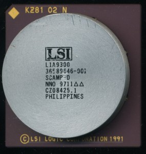
Unisys SCAMP-D - 1997 Made by LSI

Unisys SCAMP-D – 1997 Made by LSI

Burroughs Corporation started in 1886, making it the oldest computation company still in existence.  In September 1986, Burroughs merged with Sperry Corporation (of UNIVAC fame) to form Unisys which exists to this day. The story of the SCAMP though begins in 1961, with the introduction of the Burroughs B5000 mainframe.  Burroughs was a bit late to the mainframe market, but entered it with a computer that was rather ahead of its time.  The B5000 was a stack based design, and designed from the get go with the programmer in mind, it was designed with software implementation (namely the high level languages ALGOL and COBOL) in mind, rather then wrapping software around hardware design.  This made it easy to program, and thus allowed Burroughs to take customer from IBM, who released the System/360 shortly thereafter.

In 1969 the B6500 was released, improving on the design and with it the MCP (Master Control Program).  MCP was Burroughs operating system, and what came to define their machines for the decades to come.  The B6000 line (like the B5000) was a 48-bit architecture.  In addition to the 48-bit data size was a 3-bit tag that told the system what that data was, code, data, type, etc.  This simplified the instruction set greatly as instruction need not be specific to each data type, they could check the tag and know what type of data.  Coincidentally this also allowed for greater security as well, many of the buffer overflow exploits we have seen in the modern day were not possible on a Burroughs, the tag did not allow data to be executed as code, essentially it could perform as a NX flag (No Execute) such as is on modern x86 processors.

In 1984 the first A-series was released, as well as what would become ‘e-code’ a definition of the Burroughs instruction set that could be implemented in a variety of processors.  Like the DEC VAX, Burroughs wanted to clearly define the instruction set, and leave the implementation of it up to the hardware designers.  This helped ensure robust compatibility, and future proofing, ad is why MCP programs from the 70’s still can be ran today.

Read More »

Tags:
,

Posted in:
CPU of the Day

April 9th, 2015 ~ by admin

The e2v PowerPC and HiTCE Packages

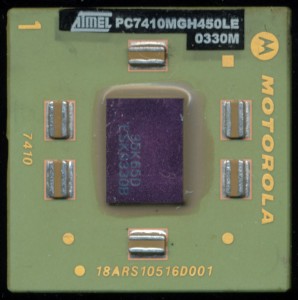
Atmel PC7410MGH450LE - Motorola Marked Package

Atmel PC7410MGH450LE – Motorola Marked Package – 2003

In the 1970’s second sources were quite important in the processor industry.  They provided a stable supply of a designed in part if the primary manufacturer (which often only had a fab or 2) had problems.  They also could widen the market for the processor.  Many of these agreements were kept active for decades after, resulting in some interesting results.

Motorola licensed many of their design to SGS, which later merged with Thomson to become STMicroelectronics. though the Thomson name was still used.  Thomson license built most of Motorola’s product line, as well as many high reliability versions.  In 1999 Atmel bought Thomson-CSF Semiconductors, and continued to make Motorola products (in their Grenoble France fab), which now included Motorola’s PowerPC line as well as the 68k line of processors.  This portion of Atmel was sold to e2v (in England) in 2006, which continued to produce the Motorola (now spun off as Freescale) PowerPC line, now branded as e2V.

The packaging used by e2v (and previously Atmel) is the same as that used by Motorola/Freescale.  The packages were custom made for Motorola/Freescale by Kyocera (and others) and so often chips with both Atmel/Motorola and e2v/Freescale markings can be found.  It is this packaging that is of interest, as it shows an interesting aspect of processor design.

Read More »

March 1st, 2015 ~ by admin

DEC Rigel: VAX Shoots for the Stars

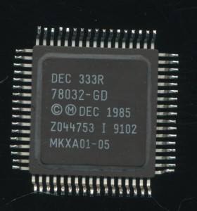
DEC 78032 DC333R MicroVAX II - 5MHz

DEC 78032 DC333R MicroVAX II – 5MHz

DEC’s 32-bit VAX architecture saw many implementations since its introduction in 1977.  Early implementations were all multi-chip, but as technology improved the VAX architecture could be implemented (at least partially) on a single VLSI chip.  The first implementation on a single chip was the MicroVAX II released in 1985.  It contained 125,000 transistors, made on a 3 micron NMOS (DEC proprietary ‘ZMOS’) process and ran at 5MHz (200ns cycle time).

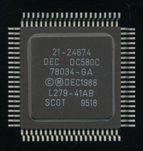
In 1987 DEC released the CVAX, the second generation VAX on VLSI.  The CVAX was made on DEC’s first CMOS process, a 2 micron design using 175,000 transistors and clocked from 10-12.5 MHz (80-10ns cycle time).  The input clock was a four-phase overlapping clock (so input frequency was 4x the cycle time, or 40-50MHz).  Performance was 2.5-3 times better then the MicroVAX II.  About half the gain was from process improvement (increased clock speed), while the rest was from architectural changes (mainly pipelining).

DEC DC580C 78034 CVAX+ 16.67MHz

DEC DC580C 78034 CVAX+ 16.67MHz

As the CVAX (and its successor the CVAX+) were released the next generation was already being designed by DEC.  This was to be Rigel.  Rigel has a 6-stage pipeline, and was made on a 2 micron CMOS process and the CPU contained 320,000 transistors, 140k of which were for logic, while the remaining 180k were for memory (cache). The separate FPU chip contained an additional 135,000 transistors.  After some early teething pains on the new CMOS process, where yields were almost non-existent, the process finally was refined enough to make commercial samples by late 1988.  The target speed for Rigel was a 40ns cycle (25 MHz clock).  This would give the Rigel a 6-8x performance gain over CVAX.  2X of this was from the process shrink (and doubling of clock speed) while 3X was from the improved pipelining.  The remainder was due to increased memory performance, not the least of which was due to Rigels 2KB of on chip cache.

Rigel, however, had other plans…

Read More »

Tags:
, , ,

Posted in:
CPU of the Day

February 22nd, 2015 ~ by admin

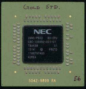
NEC SX-ACE: Quad-core Vector Supercomputing

NEC SX-ACE Processor Prototype - 2013

NEC SX-ACE Processor Prototype – 2013

When Vector computing is mentioned, the first company that comes to mind is Cray.  Cray was the leading designer and builder of vector supercomputers since the 1970’s.  Vector computing is a bit different then general purpose computing.  Simply put, a vector computer is designed to perform an instruction on a large set of data at the same time.  Such vector support has been added to x86 (in the form of SSE) as well as the PowerPC architecture (AltiVec) but they were not originally designed as such. Cray however, is not the only such company.  In 1983 NEC announced the SX architecture.  The SX-1/2 operated at up to 1.3 GFLOPs and supported 256MB of RAM per processor.  By 2001 with the SX-5 and SX-6 performance had increased to 8 GFLOPS and supported 8GB of RAM per CPU.  For a short while Cray themselves marketed and sold NEC SX computers.  Each of the processors, from SX-1 to the SX-9 was a single core processor, but with the SX-ACE, that changed.

Read More »

Tags:
, ,

Posted in:
CPU of the Day

February 13th, 2015 ~ by admin

A Forgotten 9900: The TI SBR9000

TI RAY9000C-X - SBR9000 Radiation Tolerant Processor

TI RAY9000C-X – SBR9000 Radiation Tolerant Processor

In the previous post the TI TMS/SBP9900 was covered, as well as its successor the SBP9989.  The 9989 was to be replaced by the 9989E, a 50% shrink to 2.2u.  This was never released, but TI did continue to develop the bipolar line of the 9900s.  After canceling (or perhaps just renaming?) the 9989E/9990 TI announced the SBR9000 in 1985.  The SBR9000 was a hi-speed 9989 successor fab’d on a 2 micron I2L process and clocked at 9MHz (twice the speed of the 9989).  The change in prefix from SBP to SBR hints at another feature, while the SBP9989 was a MIL-STD-883 rated part, the   SBR9000 (and its peripherals) were designed for very high radiation tolerance.  The SBR9000 was spec’d to have a total dose tolerance of 1 MegaRad (it should be noted that around 10 krads proves fatal to the average person).

The part number of this example, RAY9000C-X is a bit mysterious but there are some strong clues as to its being a prototype of the canceled SBR9000.  First of course is the 64-pin CDIP package, conveniently having 4 ground pins marked.  Pins 1,2,27 and 28 are the ground pins on all SBP9900/9989 devices.  The SBR was to be pin compatible so has the same ground pins.  The date on the back of the RAY9000 is 8525, the SBP9900 was out of production in 1983 so that rules it out, leaving either a 9989, or the most likely, a sample of a SBR9000.  Why TI canceled the SBR9000 remains a mystery, perhaps they found the 9989 to be adequate for their customers needs, as it continued to be produced into the 1990’s.

February 5th, 2015 ~ by admin

TI TMS9900/SBP9900: Accidental Success

TI TMS9900JL - 1978

TI TMS9900JL – 1978

In June 1976 TI released the TMS9900 16-bit processor.  This was one of the very first 16-bit single chip processor designs, though it took a while to catch on.  This is no fault of its own, but rather TI’s failure to market it as such.  The 9900 is a single chip implementation of the TI 990 series mini-computers.  It was meant to be a low end product and thus was not particularly well supported by TI, who did not want to cut into the higher margins of their mini-computer line.    By the late 1970’s TI began to see the possibilities of the 9900 as a general purpose processor and began supporting it with development systems, support chips, and better documentation.  If TI had marketed and supported the 9900 from its release the microprocessor market very much may have turned out a bit different.  A large portion of Intel’s success (with the 808x) was not due to a good design, but rather good support and availability.

The original TMS9900 was a 3100 gate (approx 8000 transistors) NMOS design running at up to 3MHz.  It required a 4-phase clock and 3 power supplies (5V, 12V, -5V).  It had a very orthogonal instruction set that was very memory focused, making it rather easy to program.  General purpose registers were stored off chip, with only a PC, Workspace Register (which pointed to wherever the general registers would be) and a Status Register on chip.  This made context switching fairly quick and easy.  A context switch required saving only 2-3 registers. The 9900 was packaged in a, then uncommon, and expensive, 64 pin DIP.  This allowed the full 15-bits of address and 16-bits of data bus to be available.

TI had a trick up their sleeve for the 9900 line…

Read More »

Posted in:
CPU of the Day

January 18th, 2015 ~ by admin

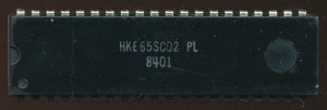
Hua Ko HKE65SC02PL – GTE Micros Asian Twin

Hua Ko CMOS 6502 - 4Mhz Industrial Temp - Direct copy from GTE Micro

Hua Ko CMOS 6502 – 4Mhz Industrial Temp – Direct copy from GTE Micro

Hua Ko Electronics was started in 1979 in Hong Kong, though with close ties to the PRC. Their story is a bit more interesting then their products, which were largely second sources of western designs. In 1980 they started a subsidiary in San Jose, CA. This was a design services center mainly ran as a foundry for other companies. They developed mask sets in their CA facility but wafer fab and most assembly was done back in Hong Kong (as well as the Philippines by 1984). Chipex also had a side business, they were illegally copying clients designs and sending them back to the PRC. In addition they were sending proprietary (and restricted) equipment back to Hong Kong and the PRC. in 1982 their San Jose facilities were raided and equipment seized. Several employees were arrested and later charged and convicted. The following investigation showed that the PRC consulate had provided support and guidance for Chipex’s operations and illegal activities. So where exactly did the HKE65SC02 design come from?

Read More »

January 16th, 2015 ~ by admin

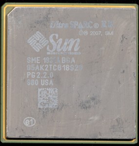
Sun UltraSPARC Rock: When is a core not a core?

Sun SME1832ABGA PG 2.2.0 UltraSPARC RK - 2007 Sample

Sun SME1832ABGA PG 2.2.0 UltraSPARC RK – 2007 Sample

In 2005 Sun (now Oracle) began work on a new UltraSPARC, the Rock, or RK for short.  The RK was to introduce several innovative technologies to the SPARC line and would complement the also in development (and still used) T-series.  The RK was to support transactional memory, which is a way of handling memory access that more closely resembles database usage (important in the database server market).  Greatly simplified, it allows the processor to hold or buffer multiple instruction results (load/stores) as a group, and then write the entire batch to memory once all had finished.  The group is a transaction, and thus the result of that transaction is stored atomically, as if it were the result of a single instruction.

The RK also was designed as a 16-core processor, with 4 sets of cores forming a cluster.  This is where the definition of a core becomes a source of much debate.  Each 4-core cluster shared a single 32KB Instruction cache, a pair of 32KB Data caches, and 2 floating point units (one of which only handled multiplies).  This type of arrangement is often called Clustered Multi-threading.  Since floating point instructions are not all the common in a database system, it made sense to share the FPU resources amongst multiple ‘cores.’

The RK was designed for a 65nm process with a target frequency of 2.3GHz, while consuming a rather incredible 250W (more power than an entire PC drew on average at the time).

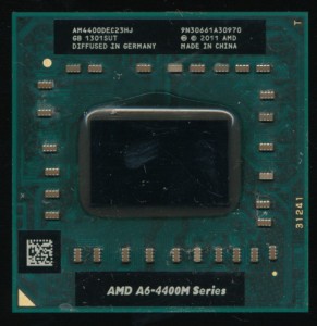
AMD A6-4400M - 2 'cores' with shared FPU and cache.

AMD A6-4400M – 2 ‘cores’ with shared FPU and cache – Piledriver Architecture

This should sound familiar, as its also the basis of the AMD Bulldozer (and later) cores released in 2011.  AMD refers to them as Modules rather then clusters, but the principle is the same.  a Module has 2 integer units, each with their own 16K data cache.  a 64K instruction cache and a single floating point unit is shared between the two.  The third generation (Steamroller) added a second instruction decoder to each module.

The idea of CMT, however, is not new, its roots go all the way back to the Alpha 21264 in 1996, nearly 10 years before the RK.  The 21164 had 2 integer ALUs and an FPU (the FPU was technically 2 FPUs, though one only handled FMUL, while the other handled the rest of the FPU instructions) .  The integer ALUs each had their own register file and address ALU and each was referred to as a cluster.  Today the DEC 21264 could very well have been marketed as a dual core processor.

The SPARC RK turned out to be better on paper then in silicon.  In 2009 Oracle purchased Sun and in 2010 the RK was canceled by Larry Ellison.  Larry Ellison, never one to mince his words said of the RK:  “This processor had two incredible virtues: It was incredibly slow and it consumed vast amounts of energy. It was so hot that they had to put about 12 inches of cooling fans on top of it to cool the processor. It was just madness to continue that project.”  While the Rock (lava rock perhaps?) never made it to market, samples were made and tested, and a great deal was learned from it.  Certainly experience that made its way into Oracle’s other T-Series processors.

December 13th, 2014 ~ by admin

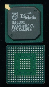
TriMedia TM-1300: VLIW Processor for the World

TiMedia TM-1300 - Marketing Sample

TiMedia TM-1300 – Marketing Sample

The roots of TriMedia start in 1987 at Philips with Gerrit Slavenburg (who wrote actual forwards for most of the Datasheets) and Junien Labrousse as the LIFE-1 processor.  At its heart it was a 32-bit VLIW (Very Long Instruction Word) processor. VLIW was a rather new concept in the 1980’s, and really didn’t catch on until the late 90’s.  Intel’s i860 could run in superscalar, or VLIW mode in 1989 but ended up a bit of a flop.  TI made the C6000 lince of the TMS320 DSP which was VLIW based.  By far thos most famous, or perhaps infamous, VLIW implementation were the Transmeta, and the Itanium, both of which proved to be less then successful in the long run (though both ended up finding niche markets).

TriMedia, released their first commercial VLIW product in 1997, the TM1000.  As the name suggests, TriMedia Processors are media focused.  They are based around a general purpose VLIW CPU core, but add audio, video and graphics processing.  THe core is decidedly not designed as a standalone processor.  It implements most CPU functions but not all, for example, it supports only 32-bit floating point math (rather than full 64 or 80 bit).

The TM-1300 was released in 1999 and featured a clock speed of 166MHz @ 2.0V on a 0.25u process.  At 166MHz the TM-1300 consumed about 3.5W, which at the time was relatively low.  It had 32K of Instruction Cache and 16K of Data Cache. As is typical of RISC processors the 1300 had 128 general purpose 32-bit registers. The VLIW instruction length allows five simultaneous operations to be issued every clock cycle. These operations can target any five of the 27 functional units in the processor, including integer and floating-point arithmetic units and SIMD units.

The above picture TM-1300 was a marketing sample handed out to the media during the Consumer Electronics Show for the processors release in 1999.  It is marked with the base specs of the chip as well as CES SAMPLE.  Likely these were pre-production units that didn’t meet spec or failed inspection, remarked for media give-aways.

Read More »

Posted in:
CPU of the Day