Archive for the 'Processor News' Category

March 6th, 2015 ~ by admin

Dawn to Ceres: Processors for the Protoplanet

Dawn's mission: Ceres

Dawn’s mission: Ceres

Dawn was launched in 2007 by NASA/JPL and was built by Orbital Sciences becoming their first interplanetary spacecraft.  Dawns mission was to visit the two largest dwarf planets in the Asteroid belt, Vesta and Ceres.  After visiting Vesta for over a year in 2011-2012 Dawn used its ion engines to break orbit, and travel to Ceres, a journey of 2.5 years.

In the next few hours Dawn will be captured by Ceres gravity and begin orbiting it.  These protoplanets, are very interesting scientifically as they provide a look into our solar systems past.  Dawn will orbit Ceres for several years and perhaps discover what the mysterious bright spots are, among other things.  Studying a planet, even a dwarf planet, requires processing power, and for that Dawn is well equipped.

Dawn is solar powered, so power budgets are of great concern.  At 3AU (three times further from the sun then Earth) Dawns solar panels are rates at about 1300 Watts.  This has to run all the science experiments, the main computers, the comms, and most importantly the electric ion engine, which uses electricity generated from the panels to excite and eject Xenon gas at very high velocities.  Thus, power consumption is more important then raw processor power here, especially for the systems that are on most of the time.

Read More »

Tags:
,

Posted in:
Processor News

November 15th, 2014 ~ by admin

Apple A8X Processor: What does an X get you?

Anandtech has an excellent article on the new Apple A8X processor that powers the iPad Air 2.  This is an interesting processor for Apple, but perhaps more interesting is its use, and the reasoning for it.  Like the A5X and A6X before it (there was no A7X) it is an upgrade/enhancement from the A8 it is based on.  In the A5X the CPU was moved from a single core to a dual core and the GPU was increased from a dual core PowerVR SGX543MP2 to a quad-core PowerVR SGX543MP4.  The A6X kept the same dual core CPU design as the A6 but went from a tri-core SGX543MP3 to a quad core SGX554MP4.  Clock speeds were increased in the A5X and A6X over the A5 and A6 respectively.

The A8X continues on this track.  The A8X adds a third CPU core, and doubles the GX6450 GPU cores to 8.  This is interesting as Imagination Technologies (whom the GPUs are licensed from) doesn’t officially support or provide an octa-core GPU.  Apple;s license with Imagination clearly allows customization though.  This is similar to the ARM Architecture license that they have.  They are not restricted to off the shelf ARM, or Imagination cores, they have free reign to design/customize the CPU and GPU cores.  This type of licensing is more expensive, but it allows much greater flexibility.

This brings us to the why.  The A8X is the processor the the newly released iPad Air 2, the previous iPad air ran an A7, which wasn’t a particularly bad processor.  The iPad Air 2 has basically the same spec’s as the previous model, importantly the screen resolution is the same and no significantly processor intense features were added.

When Apple moved from the iPad 2 to the iPad (third gen) they doubled the pixel density, so it made sense for the A5X to have additional CPU and GPU cores to handle the significantly increased amount of processing for that screen. Moving from the A7 to the A8 in the iPad Air 2 would make clear sense from a battery life point of view as well, the new Air has a much smaller batter so battery life must be enhanced, which is something Apple worked very hard on with the A8.  Moving to the A8X, as well as doubling the RAM though doesn’t tell us that Apple was only concerned about battery life (though surely the A8X can turn on/off cores as needed).  Apple clearly felt that the iPad needed a significant performance boost as well, and by all reports the Air 2 is stunningly fast.

It does beg the question though? What else may Apple have in store for such a powerful SoC?

November 12th, 2014 ~ by admin

Here comes Philae! Powered by an RTX2010

Comet 67P/Churyumov–Gerasimenko - Soon to have a pair of Harris RTX2010 Processors

Comet 67P/Churyumov–Gerasimenko – Soon to have a pair of Harris RTX2010 Processors

In less then an hour (11/12/2014 @ approx 0835 GMT) 511,000,000 km from Earth the Philae lander of the Rosetta mission will detach and begin its decent to a comets surface.  The orbiter is powered by a 1750A processor by Dynex (as we previously discussed).  The lander is powered by two 8MHz Harris RTX2010 16-bit stack processors, again a design dating back to the 1980’s.  These are used by the Philae CDMS (COmmand and Data Management System) to control all aspects of the lander.

All lander functions have to be pre programmed and executed by the CDMS with absolute fault tolerance as communications to Earth take over 28 minutes one way.  The pair of RTX2010s run in a hot redundant set up, where one board (Data Processing Unit) runs as the primary, while the second monitors it, ready to take over if any anomaly is detected.  The backup has been well tested as on each power cycle of Philae the backup computer has started, then handed control over to the primary.  This technically is an anomaly, as the CDMS was not programmed to do so, but due to some unknown cause it is working in such a state.  The fault tolerant programming handles such a situation gracefully and it will have no effect on Philae’s mission.

Why was the RTX2010 chosen?  Simply put the RTX2010 is the lowest power budget processor available that is radiation hardened, and powerful enough to handle the complex landing procedure.  Philae runs on batteries for the first phase of its mission (later it will switch to solar/back up batteries) so the power budget is critical.  The RTX2010 is a Forth based stack processor which allows for very efficient coding, again useful for a low power budget.

Eight of the instruments are also powered by a RTX2010s, making 10 total (running at between 8-10MHz).  The lander also includes an Analog Devices ADSP-21020 and a pair of 80C3x microcontrollers as well as multiple FPGAs.


October 15th, 2014 ~ by admin

Has the FDIV bug met its match? Enter the Intel FSIN bug

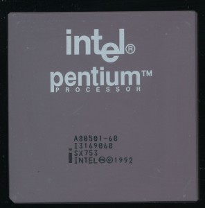
Intel A80501-60 SX753 - Early 1993 containing the FDIV bug

Intel A80501-60 SX753 – Early 1993 containing the FDIV bug

In 1994 Intel had a bit of an issue.  The newly released Pentium processor, replacement for the now 5 year old i486 had a bit of a problem, it couldn’t properly compute floating point division in some cases.  The FDIV instructions on the Pentium used a lookup table (Programmable Logic Array) to speed calculation.  This PLA had 1066 entries, which were mostly correct except 5 out of the 1066 did not get written to the PLA due to a programming error, so any calculation that hit one of those 5 cells, would result in an erroneous result.  A fairly significant error but not at all uncommon, bugs in processors are fairly common.  They are found, documented as errata, and if serious enough, and practical, fixed in the next silicon revision.

What made the FDIV infamous was, in the terms of the 21st century, it went viral.  The media, who really had little understanding of such things, caught wind and reported it as if it was the end of computing.  Intel was forced to enact a lifetime replacement program for effected chips.  Now the FDIV bug is the stuff of computer history, a lesson in bad PR more then bad silicon.

Current Intel processors also suffer from bad math, though in this case its the FSIN (and FCOS) instructions.  these instructions calculate the sine of float point numbers.  The big problem here is Intel’s documentation says the instruction is nearly perfect over a VERY wide range of inputs.  It turns out, according to extensive research by Bruce Dawson, of Google, to be very inaccurate, and not just for a limited set of inputs.

Interestingly the root of the cause is another look-up table, in this case the hard coded value of pi, which Intel, for whatever reason, limited to just 66-bits. a value much too inaccurate for an 80-bit FPU.

May 28th, 2014 ~ by admin

Intel Joins Forces with Rockchip – ARM Meets x86

rockchip logoIt’s well known that Intel missed the jump on tablet and phone processors.  Intel sold off their PXA line of ARM processors to Marvell in 2006, in an attempt to ‘get back to the basics.’  It turned out that this sale perhaps was a bit premature, as the basics ended up being mobile, and mobile is where Intel struggled (by mobile we mean phones/tablets, not laptops, which Intel has no problems with).

In January of 2011 Intel purchased the communications division of Infineon, gaining a line of application and baseband processors, based on ARM architecture of course.  Intel developed this into the SoFIA applications processor, which was ironically fab’d by TSMC.   Eventually the designs would be ported to Intel 14nm process, or that was the plan.

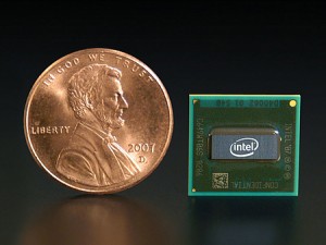
Intel Atom - Now by Rockchip?

Intel Atom – Now by Rockchip?

So this weeks announcement that Intel has signed an agreement with the Chinese company Rockchip, to cooperate on mobile applications processors is a bit of a surprise, but the details show that it makes sense.  Rockchips current offerings are ARM based, much as Intel’s current SoFIA processor, as well as Apple Ax series, Qualcomm’s SnapDragon, TI’s OMAP, etc. However, the agreement with Rockchip is not about ARM, its about x86.  For the first time in many years Intel has granted another company an x86 license, specifically, Intel will help ROckchip build a quad-core Atom based x86 processor with integrated 3G modem.  Rockchip currently uses TSMC as their fab, however also with this agreement Rockchip gets access to Intel 22nm and 14nm fab capacity.

Who wins?

Read More »

February 27th, 2014 ~ by admin

The Unlikely Tale of How ARM Came to Rule the World

Bloomberg Business Week recently published an interesting article on ARM’s rise to power in the processing world.  There first major design ‘win’ was a failed product known as the Apple Newton, yet they would go on to become a powerhouse that is no challenging Intel.

In ARM’s formative years, the 1990’s, the most popular RISC processor was the MIPS architecture, which powered high end computers by SGI, while Intel made super computers (the Paragon) based on another RISC design, the i860.  Now, nearly 2 decades later, after Intel abandoned their foray into the ARM architecture (StrongARM and X-Scale) RISC is again challenging Intel in the server market, this time, led by ARM.

MIPS, now owned by Imagination, is again turning out new IP cores to compete with ARM, and other embedded cores.  Their Warrior class processors are already providing 64-bit embedded processing power, though with a lot less press that the likes of Apple’s A7.

Tags:
,

Posted in:
Processor News

January 20th, 2014 ~ by admin

Welcome Back Rosetta: The Dynex MAS31750 Awakens

Rosetta Comet Chaser - Dynex 1750

Rosetta Comet Chaser – Dynex 1750

The ESA’s comet chaser Rosetta has just today awoken from a long deep sleep on its comet chasing (and landing) mission.  The solar powered spacecraft was launched back in 2004.  It is based on the Mars Mariner II (itself based on the Voyager and Galileo) spacecraft design of the early 1990s (when the mission was first conceived.)  Main differences include using very large solar arrays versus a RT (Radioisotope Thermal Generator) and upgraded electronics.

In order to conserve power on its outward loop (near Jupiter’s orbit) most all systems were put to sleep in June of 2011 and a task set on the main computer to waken the spacecraft 2.5 years later and call home.  The computer in charge of that is powered by a Dynex MAS31750 16-bit processor running at 25MHz, based on the MIL-STD-1750A architecture.

A reader recently asked why such an old CPU design is still being used rather then say an x86 processor.  As mentioned above the Rosetta design was began in the 1990’s, the 1750A was THE standard high reliability processor at the time, so it wasn’t as out of date as it is now that its been flying through space for 10 years (and 10 years in the clean room).  The 1750A is also an open architecture, no licenses are or were required to develop a processor to support it (unlike x86). Modern designs do use more modern processors such as PowerPC based CPUs like the RAD750 and its older cousin the RAD6000.  Space system electronics will always lag current tech due to the very long lead times in their design (it may be 10 years of design n the ground before it flies, and the main computer is selected early on).  x86 is used in systems with 1) lots of power, and 2) somewhat easily accessible.  Notably the International Space Station and Hubble.  x86 was not designed with high reliability and radiation tolerance in mind, meaning other methods (hardware/software) have to be used to ensure it works in space.

Currently the ESA designs with an open-source processor known as the LEON, which is SPARC-V8 based.

November 19th, 2013 ~ by admin

MAVEN To Mars: Another BAE RAD750 CPU

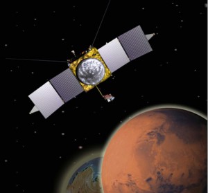
MAVEN to Mars - RAD750 Powered

MAVEN to Mars – RAD750 Powered

NASA has successfully launched the $671 million MAVEN mission to Mars for atmospheric research.  Like the Mars Reconnaissance Orbiter it is based on, it’s main computer is a BAE RAD750,  a radiation hardened PowerPC 750 architecture.  This processor first flew on the Deep Impact Comet chaser and is capable of withstanding up to 1 million rads of radiation.  The entire processor sub-system can handle 200,000 rads.  To put this in perspective, 1000 rads is considered a lethal dose for a typical human.  Likely much higher then a Apple Mac G3 that the PowerPC 750 was originally used in back in 1998 as well.   The processor can be clocked at up to 200MHz though often will run slower for power conservation.

The MAVEN should reach Mars within a few days of the Indian Space Agency’s $71 million Mangalyaan Orbiter launched earlier this month.  MAVEN is taking a faster route, at the expense of a heavier booster and larger fuel consumption.  The Mangalyaan Orbiter’s main processor is the GEC/Plessey (Originally produced by Marconi and now Dynex) MAR31750, a MIL-STD-1750A processor system.

November 17th, 2013 ~ by admin

Itanium is Dead – And other Processor News

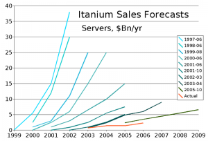
Itanium Sales Forecasts vs Reality

Itanium Sales Forecasts vs Reality

‘Itanium is dead’ is a phrase that has been used for over a decade, in fact many claimed that the Itanium experiment was dead before it even launched in 2001.  The last hold-out of the Itanium architecture was HP, likely because the Itanium had a lot in common with its own PA-RISC.  However HP has announced that they will be transitioning their NonStop sever series to x86, presumably the new 15-core Xeons Intel is developing.  Itanium was launched with goal of storming the server market, billed as the next greatest thing, it failed to make the inroads expected, largely due to the 2 decades of x86 code it didnt support, and poor initial compiler support.  Many things were learned from Itanium so though it will become but a footnote, its technology will live on.

Interestingly other architectures that seemed to be n the brink are getting continued support in new chips.  Imagination, known for their graphics IP, purchased MIPS, and now has announced the MIPS Warrior P-class core.  This core supports speeds of over 2GHz, and is the first MIPS core with 128 bit SIMD support.

Broadcom, historically a MIPS powerhouse, has announced a 64-bit ARM server class processor with speeds of up to 3GHz. Perhaps ironic that ARM is now being introduced into a market that Itanium was designed for. Broadcom has an ARM Architecture license, meaning they can roll their own designs that implement the ARM instruction set, similar to Qualcomm and several others.

POWER continues to show its remarkable flexibility.  Used by IBM in larger mainframes in the POWER7 and POWER8 implementations it crunches data at speeds up to 4.4GHz.  On the other end of the spectrum, Freescale (formerly Motorola, one of the developers of the POWER architecture) has announced the 1.8GHz quad-core QorIQ T2080 for control applications such as networking, and other embedded use.  These days the POWER architecture is not often talked about, at least in the embedded market, but it continues to soldier on and be widely used.  LSI has used it in their Fusion-MPT RAID controllers, Xilinx continues to offer it embedded in FPGAs and BAE continues to offer it in the form of the RAD750 for space-based applications.

Perhaps it is this flexibility of use that has continued to allow architectures to be used.  Itanium was very focused, and did its one job very well. Same goes for the Alpha architecture, and the Intel i860, all of which are now discontinued.  ARM, MIPS, POWER, x86 and a host of MCU architectures continue to be used because of their flexibility and large code bases.

So what architecture will be next to fall? And will a truly new architecture be introduced that has the power and flexibility to stick around?

Tags:
, , ,

Posted in:
Processor News

September 18th, 2013 ~ by admin

Hold the Phone – Why Intel Making the A7 Might Not Be Awesome – Updated

Update: Sept 20th: It has been confirmed that the A7 is still made by Samsung, most likely on their 28nm High-k dielectric process (same as the Exynos in the Galaxy S5). The M7 has also been confirmed to be an off the shelf NXP LPC1800 ARM Cortex-M3, running at up to 180MHz, nothing spectacular, and fairly common for sensor interface.  What does this mean for Apple? It means if they can get that much performance out of Samsung’s 28nm process, when and if they Do switch to Intel, the possibilities are quite interesting.

However, its still interesting to play what if, so the below analysis remains.
It has been rumored that Apple’s new A7 processor may be fab’d by Intel, rather then TSMC and Samsung.  Previous generations of the Ax have been fab’d by Samsung and in July it was announced that TSMC had picked up an Apple contract.  Intel has in the last year begun to market, albeit quietly its excess fab capacity.  This is an entirely smart move by Intel.  It will help them use their multi-billion dollar fabs to the fullest capacity, as well as test and experiment with other designs.

Apple using Intel as a contract fab makes sense, for Apple.  Intel has the best fab technology in the world, bar none.  Apple is less concerned with competing on price, than they are making the best devices possible.  To have the best devices you need the best (fastest and lowest power) chips.  To have the best chips you need the best processes, and that means Intel.  None of this is in question.  If the A7 is fab’d by Intel it will greatly help Apple attain its market leading position.  However, what is in question is whether this is a ‘huge win’ for Intel.  One blog even referred to Intel making Apple chips as “That’d be a hell of a score for Intel.”  In reality this will have little benefit to Intel.  Certainly not financially. Lets look at why.

Read More »

Posted in:
Processor News