Archive for the 'Research' Category

November 1st, 2013 ~ by admin

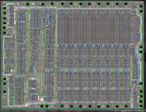
nCube and the Rise of the HyperCubes

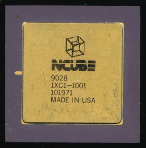
nCube/2 Processor - 20MHz The logo is a tesseract - 4-way Hypercube

nCube/2 Processor – 20MHz
The logo is a Tesseract – a 4-way Hypercube

In 1983 Stephen Colley, Dave Jurasek, John Palmer and 3 others from Intel’s Systems Group left Intel, frustrated by Intel’s seeming reluctance to enter the then emerging parallel computing market.  They founded a company in Beaverton, Oregon known as nCube with the goal of producing MIMD (Multiple Instruction Multiple Data) parallel computers.  In 1985 they released their first computer, known as the nCube/10.  The nCube/10 was built using a custom 32-bit CMOS processor containing 160,000 transistors and running initially at 8MHz (later increased to 10).  IEEE754 64-bit floating point support  (including hardware sqrt) was included on chip.  Each processor was on a module with its own 128KB of ECC DRAM memory (implemented as 6 64k x 4 bit DRAMs.)  A full system, with 1024 processor nodes, had 128MB of usable memory (160MB of  DRAM counting those used for ECC).  From the outset the nCube systems were designed for reliability, with MTBFs of full systems running in the 6 month range, extremely good at the time.

The nCube/10 system was organized in a Hypercube geometry, with the 10 signifying its ability to scale to a 10-way Hypercube, also known as a dekeract.  This architecture allows for any processor to be a maximum of 10-hops from any other processor.  The benefits are greatly reduced latency in cross processor communication.  The downside is that expansion is restricted to powers of 2 (64, 128, 256, 512 etc) making upgrade costs a bit expensive as the size scaled up.  Each processor contained 22 DMA channels, with a pair being reserved for I/O to the host processor and the remaining 20 (10 in + 10 out) used for interprocessor communication.  This focus on a general purpose CPU with built in networking support is very similar to the Inmos Transputer, which at the time, was making similar inroads in the European market.  System management was run by similar nCube processors on Graphics, Disk, and I/O cards.  Programming was via Fortran 77 and later C/C++. At the time it was one of the fastest computers on the planet, even challenging the almighty Cray.  And it was about to get faster.

Read More »

March 2nd, 2013 ~ by admin

Chuck Moore: Part 2: From Space to GreenArrays

Part 2 of my abbreviated biography of Chuck H. Moore’s processor designs.  Part 1 covered the early days of Novix, and the RTX2000.

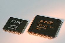
Patriot Scientific IGNiTE - Based on the Sh-Boom

Patriot Scientific IGNiTE – Based on the Sh-Boom

Moore was not content to just create one processor design, or one company.  In the 1980’s he also ran Computer Cowboys, a consulting/design company.  In 1985 he designed the Sh-boom processor with Russell H. Fish III.  This was a 32-bit stack processor, though with 16 general purpose registers, that was again designed with Forth in mind.  It was capable of running much faster then the rest of the system so Moore designed a way to run the processor faster then the rest of the board, and still keep things in sync, innovative at them time, and now standard practice.  The Sh-Boom was not a particularly wide success and was later licensed by Patriot Scientific through a company called Nanotronics, which Fish had transferred his rights to the Sh-Boom to in 1991.  Patriot rebranded and reworked the Sh-Boom as the PSC1000 and targeted it to the Java market.  Java byte code could be translated to run in similar fashion as Forth on the PSC1000 and at 100MHz, it was quick.  In the early 2000’s Patriot again rebranded the ShBoom and called the design IGNITE.  Patriot no longer makes or sells processors, concentrating only on Intellectual Property (Patent licensing).

After designing the Sh-Boom, and the Novix series, Moore developed yet another processor in 1990 called the MuP21.  This was the beginning of a what would be a common thread in Moore’s designs.  MISC (Minimal Instruction Set Computer), which is essentially an even simpler RISC design, multiprocessor/multicore, and efficiency have become the hallmarks of his designs.  The MuP21 was a 21 bit processor with only 24 instructions. At 20MHz performance was 80 MIPS as it could fetch four 5-bit instructions in a 20 bit word.  It was manufactured in a 40 pin DIP on a 1.2 micron process with 7000 transistors.

iTvcIn 1993 Moore designed the F21, again a 21 bit CPU based on the MuP21, designed to run Forth, and including 27 instructions.  It was fab’d by Mosis on a 0.8u process.  The F21 microprocessor contains a Stack Machine CPU (with a pair of stacks like the NC4000), a video i/o coprocessor, an analog i/o coprocessor, a serial network i/o coprocessor, an parallel port, a real time clock, some on chip ROM  and an external memory interface. Performance was 500 MIPS (this was an asynchronous design, so ‘clock speed’ is a bit of a misnomer) and transistor count had risen to about 15,000.  The F21 was made up through 1998, however the design continued to evolve.  A version of the F21 was developed called the i21, originally for Chuck Moore’s iTV Corporation, which was one of the very first set top Internet appliance companies.  It integrated additional featured such as infrared remote interface, modem DMA interface and a keyboard DMA interface. The F21 scaled well, and was tiny, remember, only 15,000 transistors, which at 0.18u takes up a VERY small die, and allowed performance to hit 2400MIPS @ 1.8V.  One could put a very large amount of these on a single die…..

Read More »

Tags:

Posted in:
Research

February 21st, 2013 ~ by admin

Charles Moore: From FORTH to Stack Processors and Beyond

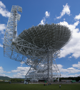
NRAO Radio Telescope

NRAO Radio Telescope

There are many greats of the CPU industry, some, such as Federico Faggin (designer of the 4004 and worked on the 8008, then founded Zilog) are fairly well known.  Others include Gelsinger and Meyer (of x86 fame) perhaps even Gordon Moore, of which a  ‘law’ is named.  Chuck Peddle and Bill Mensch designed the ubiquitous 6502 processor, but there were more, many more. Engineers whose names have been oft forgotten, but whose work has not.  The 1970’s and 80’s were the fast and the furious of processor designs.  Some designs were developed, sold, or canceled in weeks, months; years were not a period of time that was available to these designers, for in a year, a new technology would dictate a new design.

One of these designers is Charles H. Moore. (aka Chuck Moore).  Chuck is perhaps best known for inventing the FORTH programming language in 1968, originally to control telescopes.  It was a stack based language, and lended itself well to small microcomputers and microcontrollers.  Some microcontrollers even embedded a FORTH kernel in ROM.  It was also designed to be able to be ported to different architectures easily.  FORTH continues to be used today for a variety of applications.  However Chuck did not just invent a 1970’s programming language.

Read More »

Posted in:
Research

January 12th, 2013 ~ by admin

The Intel 80186 Gets Turbocharged – VAutomation Turbo186

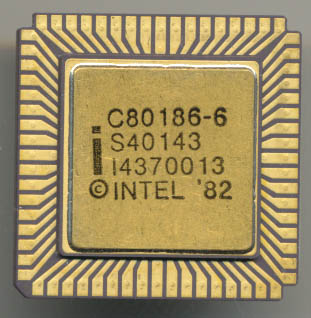
Original Intel 6MHz 80186 Made in 1984

Original Intel 6MHz 80186 Made in 1984

2012 marked the 30th anniversary of the introduction of the Intel 80186 and 80188 microprocessors.  These were the first, and arguably only, x86 processors designed from the beginning as embedded processors.  It included many on-chip peripherals such as a DMA channels, timers and other features previously handled by external chips.  Initially released at 6MHz, clock for clock many instructions were faster then the 8086 it was based on, due to hardware improvements.

In 1987 Intel move the 186 to a CMOS process and added more enhancement including math co-processor support, power down modes and a DRAM refresh controller.  Speeds were increased up to 25MHz (from the 10MHz max of the NMOS version).  Through the years Intel continued to developed new versions of the 186 with added features, lower voltages, and different packages.  It was not until 2007 that Intel finally stopped production of the 186 series.  It continued to be made by others under license including AMD, who made versions running up to 50MHz.  Fujitsu and Siemens also produced the 186 series. Like the 8051 the 186 gained significant support, being embedded in millions of devices.  The instruction set was familiar, debugging and development systems were (and are) plentiful so the 186 core continues to be in wide use.

As IC complexity and transistor counts increased the need for a processor core that could not just be embedded into a system, but be embedded into a custom ASIC or SoC became apparent. IC’s were being designed to handle things like DVD playback, set-top boxes, flat panel control and more.  These applications still required some sort of processor to handle them but having to have a separate IC for it was not economical.

pixelworks PW166B - 67MHz Tubro186 based Flatpanel Controller made in 2004

pixelworks PW166B – 67MHz Tubro186 based Flatpanel Controller made in 2004

VAutomation (founded in 1994) designed Verilog and VHDL synthesizable cores (meaning they could be ‘dropped’ into an IC design or FPGA).  In November 1996 VAutomation licensed the 8086/8, 80186/8 and the CMOS versions from Intel.   This gave them them ability to design their own compatible models of these processors without fear of litigation.  More importantly it allowed them to sub-license these designs to others.  In 1997 VAutomation demo’d their first 186, the V186 core.  This was a Intel 80186 compatible core that could be synthesized into a customers design.  It was ‘technology independent  which means it was not restricted to a certain process or even technology.  It could be used in CMOS, ECL, 0.35u, 1 micron, whatever the client needed.  On a 0.35u CMOS process it was capable of speeds in excess of 60MHz, and did so with less then 28,000 gates. One of the first licensees was Pixelworks, which made controllers for monitors.  Typical licensing was a $25,000 fee up front and royalties on a per device basis usually split into a high volume (over 500,000 units) and low volume.  Typical price per chip was $0.25-$2.00, which was cheaper then the $15 price Intel was charging for a discrete 80C186.

Read More »

October 8th, 2012 ~ by admin

Apple A6 vs Rockchip RK3066: 4 Years vs. 6 weeks of design

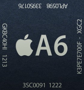
The introduction of the iPhone 5 was also the introduction of Apple’s first truly original Application Processor design.  The iPhone 2, 3G and 3GS all featured designs by Samsung.  The iPhone 4 introduced the A4, which was closely based on the Hummingbird Cortex-A8 core developed with Samsung and Intrinsity, again, not a truly Apple design.  The iPhone 4S introduced the A5 (and the A5X used in the iPad 2).  The A5 is based on the ARM Cortex-A9 MPCore, a standard ARM design, albeit with many added features, but architecturally, the processor is not original, just customized.

ARM provides cores designs for use by developers, such as the Cortex-A9, A8, etc.  These are complete designs of processors that you can drop into your system design as a block, add your own functions, such as a graphics system, audio processing, image handling, radio control, etc and you have your processor.  This is the way many processor vendors go about things.  They do not have to spend the time and effort to design a processor core, just pick one that meets their needs (power budget, speed, die area) and add any peripherals   Many of these peripherals are also licensed as Intellectual Property (IP) blocks making building a processor in some ways similar to construction with Legos.  This is not to say that this is easy, or the wrong way to go about things, it is in fact the only way to get a design to market in a matter of weeks, rather then years.  It allows for a wide product portfolio that can meet many customers needs.  The blocks are often offered for a specific process, so not only can you purchase a license to a Cortex-A9 MPCore, you can purchase one that is hardware ready for a TSMC 32nm High-k Metal Gate process, or a 28nm Global Foundries process.  This greatly reduces the amount of work needed to make a design work with a chosen process. This is what ARM calls the Processor Foundry Program.

Read More »

Tags:
, ,

Posted in:
Research

September 6th, 2012 ~ by admin

Intel vs. The World – The Infamous ‘338 Patent

A Brief History

Long before the mess of Apple vs. Samsung (and seemingly everyone else), there was another famous company, with a patent in hand, that it seemed everyone was violating.  The issue of Intellectual Property (IP), and its associated patents has long been an issue in the technology business, and certainly in the business of CPU’s.  There are many many functions inside a CPU, different structures for handling instructions, memory access, cache algorithms, branch prediction etc.  All of these are unique, intellectual property.  It doesn’t matter if you implement them with a slightly different transistor structure, as long as the end product is relatively the same, there is the risk of violating a patent.  Patents are tricky things, and litigating them can be very risky.  You must balance the desire to keep competition from violating your IP, but at the same time minimize the risk that your patent is declared invalid.  This is why most cases end up in an out of court settlement, usually via arbitration.  Actual patent jury trials are fairly rare, as they are very expensive and very risky to all parties involved

Infringing?

In the early days (1970’s and early 1980’s) there was routine and widespread cross licensing in the industry.  Many companies didn’t have the fab capacity to reliably meet demand (IBM wouldn’t purchase a device unless it was made by at least 2 companies for this very reason) so they would contract with other manufacturers to make their design.  Having other companies manufacture your design, or compatible parts, also increased the market share of your architecture (8086, 68k etc).  For years AMD made and licensed most everything Intel made, AMD also licensed various peripheral chips to Intel (notably the 9511/2 FPU).  As the market grew larger, the competition increased, Intel (and others) began to have enough reliable fab capacity to safely single source devices.  Meanwhile other companies continued to make compatible products, based on previous licensing.  AMD notably made x86 CPU’s that ate into Intel’s market share. In the 1970’s Intel had cross license agreements with AMD, IBM, National, Texas Instruments, Mostek, Siemens, NEC and many others.

Read More »

Posted in:
Research

April 21st, 2011 ~ by admin

Inside the 1802: a Visual6502.org View


RCA 1802E Die - 20x magnification - Visual6502.org

The talent at Visual6502.org continues.  After imaging and building a complete simulator for the MOS 6502 they did the same for the Motorola 6800 (from which the 6502 was based).

We have sent Visual6502.org several chips and they have now imaged the RCA 1802 that we sent.  What is very interesting is how little marking are on the die, the only that I could see was the number ‘10824.’  This particular chip was dated early 1981 though the 1802 COSMAC was designed in 1976 and was one of the first CMOS microprocessors.  The 1802 had around 5000 transistors (Visual6502 will let us know exactly how many once they are done, and of course what each and every one of them does). For higher res shots and more info see here

February 20th, 2011 ~ by admin

Russian Computers on the Buran Shuttle

In the 1970’s and the 1980’s the Soviets developed and successfully flew their own version of the Space Shuttle.  It was called the Buran.  In many ways it was an enhancements of the US Space Shuttle, based on what the Soviets saw as deficiencies in the US design.  One of the biggest differences was the piloting.  The US STS (Shuttle Transport System) was designed to be a crewed vehicle.  The computers assisted the pilot/co-pilot in launch, orbit, and recovery.  Many of the functions on the STS can be handled by the computers (the Flight Computers were based on the IBM System/4 Pi) but the pilot was needed to handle the rest.  The Soviets, on the other hand, designed the Buran to be able to launch, orbit, and land fully automatically.  This meant the computers has to be very robust, and the programming even more so.  The computers had to respond quickly to chaning inputs, and be able to handle failures gracefully.  While each mission would have a set profile, unknown conditions would cause deviations that the computers must detect, analyse, and properly handle.  Preferably without wrecking the multi-billion ruble space craft.

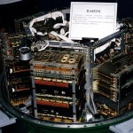
Buran Computer

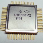
The main computer of the Buran is actually 4 independent systems that receive the same inputs.  The clock in generated externally (with 4 backups) so that each computer is in perfect time (the STS uses software to ensure the computers are in time, rather then hardware).  Redundancy is achieved by the voting system. Each computers outputs are compared, if one computers output is different, it is automatically shut down, leaving the 3 remaining computers.  These computers are powered by a clone of the DEC PDP-11.  The Soviet’s ‘acquired’ a few PDP/11 systems and then copied and cloned them into many different systems.  The most common is the 1801 a 5MHz NMOS PDP-11 type device.  The Buran used the 1806, which is the CMOS version.   Here is a general overview of the flight computer.

Angstrem CMOS N1806VM2 - MicroVAX

In addition to the 1806 there were many sub-systems with their own processors.  Details on these are a bit thin, however looking at other Soviet space computer designs it is very likely that many of these used the 134IP3 series of ALUs (a clone of the 54L181 TTL 4-bit ALU).  This chip is also used in the Argon-16 and Argon 16A computers of the Soyuz and Progress spacecraft that are still in use today.  Bit-slice devices were used extensively for many Soviet designs as it gave them a great ability to design custom processors to meet the applications needs.  The Argon-17, which was used for anti-ballistic missile work, was based on the 583 series, an 8-bi slice processor.  The C100 and C101 computers (used as weapons computers on the MiG-29) also use a BSP design.

Posted in:
Research

February 17th, 2011 ~ by admin

The AMD 2901 Bit Slicer and Second Sourcing

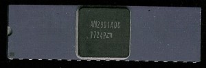
AMD AM2901ADC – 1977

In August 1975 AMD introduced the ‘100 ns Bipolar microprocessor.’ This was a bit-slice device. Essentially a 4-bit ALU (like a 74181) with functionality (scratch pad memory and accumulator register) to make it work as a processor that could be scaled to any bit width (using the 2909 sequencer and 2910 controller).  Being made in bipolar allowed for the high speed (10MHz at the time was pretty quick).  The introduction of the 2901 also marked the beginning of the end to the competition int he bit-slice arena.  A combination of marketing, second-sourcing, and a good product allowed AMD to completely dominate the bit-slice market.  Even today most bit-slice designs are based on the 2901 from 35 years ago.

At the time there were several other bit-slice processors on the market.  Intel had the 3002 (a 2-bit design), National’s IMP-8 and IMP-16, and the original TTL 74181 were all bit-slice devices.  MMI (which AMD bought in the 1980’s) had introduced the 6701 4bit slice in 1974, a full year before AMD’s 2901.  TI had the SBP0400A and Motorola the MC10800 (in ECL – 1976). So why with all this competition did AMD come to dominate?

Raytheon AM2901ADC – 1980

Second Sourcing

Second sourcing is the licensing of a design to other companies for them to manufacture, market and sell it.  Sometimes its simply a license to manufacture, sometimes it comes with technical assistance, or even complete mask sets to make the device.  There are three main reasons this is done (or was done back in the day)
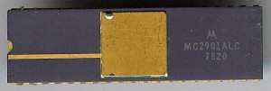
 

Guaranteed Availability.

In the 1970’s making IC’s was a relatively new process, one with many bugs, and often reliability issues.  Having a second source was a must to get a big design win. A system design would not want to design a system around a chip that may end up not being available, or not be available in the quantities needed.  Having a second source to get the IC from alleviated this problem.  It gave system designers a stable supply, regardless if the primary source could not keep up, or had a problem.
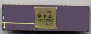
 

Distribution

Second-sourcing helped solve distribution problems as well.  A company may have an excellent design, but no way to sell it.  Often this was a geography problem.  American companies did not initially have a large presence, or distributors set up, in Europe or Japan.  An American company would often second-source a design to a European company (such as Siemens or Thomson) solely to get their design distributed in that area.
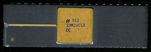
 

Marketing

One of the keys to a processors success is design wins.  It can be the best processor on the market,. but if no one uses it, it will fail.  Having additional companies make, and market the processor vastly increased its exposure.  Second-source companies would also typically make development systems, and other support tools, as well as vast documentation for the processor.  This helped ensure that engineers knew about the processor, how to use it, and whee to get it, ensuring its winning of more sockets.
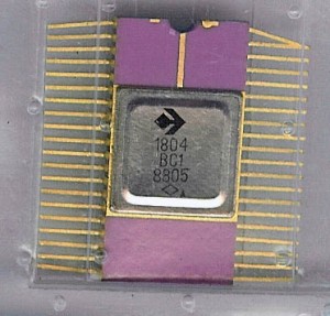
Soviet Electronika 1804VS1 – 2901 Clone – 1988

AMD clearly understood the importance of second-sourcing.  In November 1975, just months after the 2901 was released, they designed an agreement with Motorola to make the 2901.  In December, they signed up Raytheon, and in March of 1976 AMD signed an agreement with the SESCOSEM division of Thomson-CSF, to make and distribute the 2901 in markets outside the US and Japan. In June 1976 AMD amended their agreement with Motorola to include more technical assistance, ensuring Motorola could get the 2901 to market. In September 1976 MMI canceled the 6701, as they were unable to compete.  MMI had no second-sources for the 6701 which likely led to its failure.

As the years went by, AMD added more second-sources, and dropped a few. Eventually coming to completely dominate the bit-slice market.  The Soviets began to copy the 2901 around 1985 (not particularly legally but they did what they had to) and continued to do so until well into the 90’s.

Year Second Sources
1975 Motorola
1976 Motorola, Raytheon, Thomson
1977 Motorola, Raytheon, Thomson, National
1978 Motorola, Raytheon, National, Fairchild, NEC, Signetics, Thomson
1980 Motorola, Raytheon, National, Fairchild, NEC, OKI (MSM8821?), Thomson
1982 Motorola (2903), National, Fairchild, NEC, Thomson
1985 National, Thomson, Cypress, USSR
1990 Cypress, IDT, Thomson, National, USSR
1995 Cyrpress, IDT, WSI, Thomson, Russia

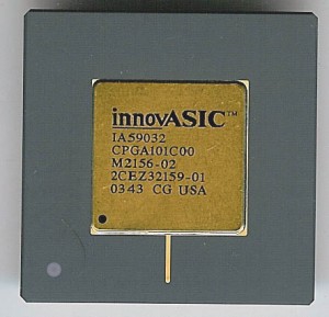
Innovasic IA59032 – 8 x 2901 – 2003

AMD also made the AM29C101 which was 4 2901s in a single chip, producing a 16bit processor.  Cypress manufactured a copy of the 29C101 called the CY7C9101

Several other companies also designed multiple 2901s into a single chip. WSI (and later InnovASIC) designed the 59032, which has the equivalent of 8 2901s to form a 32 bit slice and the 59016 which was  16bit slice (4x 2901).  IDT designed the 49C402 which was also a 16 bit slicer.  Today the 2901 is still in wide use, and while not generally used for new designs, it still powers a vast amount of electronic equipment that still is in use.  InnovASIC still manufactures the 2901 (in 59032 form) to this day.

Posted in:
Research

February 5th, 2011 ~ by admin

Atmel Buys MHS, Again – The Twisted History of Atmel, Temic and MHS

Today Atmel purchased MHS Electronics, a French company.  Why is this interesting? Because this is not the first time Atmel has bought MHS, in one form or another.  Atmel, Matra, MHS, and Temic’s histories are rather intertwined, with mergers, acquisitions and name changes occurring frequently over the last 25 years.

A Bit of History….

Atmel 4Mbit EPROM - 1995

Atmel was founded in 1984 by George Perlegos, a former Intel employee, as a fab-less semiconductor company.  Originally Atmel designed EPROM’s and PLDs.  They were manufactured by Sanyo, which had an Intel license.  Intel, however, sued Atmel (along with Hyundai, iCT, AAS, Cypress, and Pacesetter Electronics) over EPROM patents in 1987.  The courts sided with Intel which severely hampered Atmel’s ability to make EPROM’s.  Their focus then switched to non-volatile memories, such as Flash for which they have become very well known and continue to make.  In 1989 they bought their own fab (from Honeywell) in Colorado Springs, CO and in 1993 released an 8051 (Intel licensed) with integrated Flash memory.  This catapulted Atmel into the microcontroller market that is today one of their core businesses.  In 1994 Atmel Purchased SEEQ, an EPROM and EEPROM company that Perlegos helped start in 1981.  In 1995 Atmel opened a fab in Rousset, France, thus beginning the French connection.

Temic 80C32 - 1998

Temic had its beginning in 1903 as Telefunken (Ironically a joint venture of Siemens and another company).  In 1967 AEG merged with Telefunken and in 1985 Daimler-Benz bought Telefunken-AEG and renamed it to simply AEG. The semiconductor division of AEG was then called TEMIC (TElefunken MICroelectronics).  In 1998 AEG sold TEMIC to Vishay, another automotive electronics supplier.  Vishay only had interest in the discrete and power electronics portions so immediately sold the IC portion to Atmel. This gave Atmel a Bipolar fab in Germany

Matra Harris Semiconductors SA (MHS) was created in 1979 as a joint venture between Matra, the French high technology group, and Harris Semiconductor, an American semiconductor manufacturer. In 1989, Harris withdrew from the partnership, and the name was changed to Matra MHS SA. Two years later, AEG (The electronics division of Daimler-Benz) purchased 50% of Matra and merged the unit with its TEMIC Semiconductor subsidiary. In 1998, AEG purchased the remaining shares of the company and the name was changed again, to MHS SA.

MHS 80C52 - 1988

This was part of the sale to Vishay mentioned above, which Atmel then purchased.  MHS had one CMOS fab in Nantes, France which was included in the sale

Here is where it gets complicated…

The result of all of this was Atmel now owned Temic, MHS, 2 fabs in France, one in Germany, their original fab in Colorado as well as a fab in England, and one in Texas.  Atmel needed to consolidate their fabs so in 2005 they sold the MHS fab in Nantes France to Xbybus, a French company. Xbybus ran the Nantes fab as MHS Electronics.  In 2008 Atmel sold their fab in Germany (the former TEMIC fab) to Tejas semiconductor.  This left Atmel with one fab in Colorado, and one in Rousset, France.  Labor issues at the French fab in regards to Atmel’s need to reduce production led to indefinite strikes at this fab, hampering Atmel’s work to sell it.  Finally in 2010 Atmel received approval from the French gov’t to sell the fab to LFoundry, a French company.  This marked the end of Atmel’s fab presence in France…..

Telefunken U3870M CPU (Mostek Clone) - 1986

For about 9 months…

Today, Atmel has bought MHS Electronics, and their fab in Nantes, France, a fab they owned from 1998-2005.  MHS had been having financial troubles since 2008.  An interesting end to a series of event that began over 30 years ago.

I suspect though that we have not yet heard the last of MHS, or perhaps TEMIC.