Archive for the 'Research' Category

February 2nd, 2011 ~ by admin

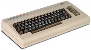
How many Commodore 64 computers were really sold?

Production numbers of vintage technology have always been a somewhat mysterious subject.  How many 4004 processors did Intel actually make? I am not even sure Intel knows.  Unlike modern car companies who can track production numbers down to the shift of the day it was made, computer companies of the 70’s and 80’s were rather fast and loose with record keeping.

Thankfully with some research, serial numbers and some math (the famous tank equation) Michael Steil of Pagetable.com came up with what appears to be a very good estimate of Commodore 64 production.  12.5 million units, somewhat less then other numbers that have been thrown around, but backed by research and supported by math.  Read how he came to the conclusion here.

Tags:
,

Posted in:
Research

November 16th, 2010 ~ by admin

The History of the SMS300 and Signetics 8X300 Processors

On November 20th, 1969 a small company was formed in Mountain View, CA called Scientific Micro Systems Inc (SMS). They would join the dozens of post-Fairchild semiconductor startups in Silicon Valley.  Many of these we remember and know well, Intel, AMD, Zilog, MOS all are familiar and have designed processors that left a story, if not a legacy, in history. SMS has became a forgotten player in the roaring 70’s but they did introduce a few important things to the market. First 4096-bit bipolar Schottky ROM? SMS. First 256-bit bipolar Schottky RAM? Again SMS.

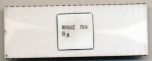
Signetics N8X300I – Early 1978

In January 1975 SMS announced prototypes of their own 8-bit microcontroller.  The SMS300 was a non-traditional design.  It focused on manipulation of signals.  It had 16-bit instructions, but operated on data 8 bits at a time.  It had very limited ways of accessing external memory (and no real way to access data memory).  It was designed as perhaps the first DSP.  It was fabricated in bipolar Schottky transistor technology.  This allowed it to be incredibly fast (albeit very power hungry) for its time.  Initial clock speeds were 6.66MHz and quickly ramped to 8MHz in 1976.  The SMS300 was initially not available for sale as a single chip.  It was sold as a single board computer called the SMS330 (as well as the SMS331 and SMS332) which contained everything needed to run the SMS300.  This was packaged like a oversized 64pin DIP (similar to how some of the BASIC Stamp microntrollers are today). These systems started at $370 and topped out at $1460.  In August of 1975 SMS ‘unbundled’ the SMS300 and began selling it (and its support chips) separately to those who wanted them.

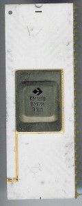
Soviet Electronika KM1818VM01A 8X300 Clone

Soviet Electronika KM1818VM01A 8X300 Clone

SMS did not make the SMS300 themselves, they contracted another Silicon Valley company to fabricate them.  Signetics, founded in 1961 by ex-Fairchild workers, was the first company founded to solely manufacture ICs rather then discrete transistors.  In 1975 Signetics was purchased by Philips but continued to operate under the Signetics trademark until 1993. Signetics made all of the SMS300 devices for SMS, and in 1976 Signetics became a second-source, and could sell the SMS300 under the Signetics brand.  By 1978 Signetics had purchased the rights to the SMS300 and renamed it the 8X300.  1977 or 1978 is generally when people think the 8X300 was develped. This is, unfortunately, due to forgotten history as by the time Signetcs bought the design, it had been on the market and in use for over 2 years.  Signetics continued to make the 8X300 into the early 1990s where it found wide use in disk controllers, telecommunications and other DSP like environments.  The N8X300 was also second sourced by AMD though I have yet to see one.  The 8X300 was also *second sourced* by the Soviets in the 80’s and early 90’s by the Electronika state electronics company in what is now Voronezh, Russia.  These of course were not licensed copies but they are however, still of interest.

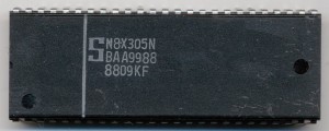
Signetics N8X305N Early 1988

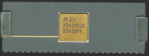
In around 1982 Signetics released the N8X305, the successor to the 8X300.  It was functionally compatible but increased the general purpose registers to 13 from 8 among some other instruction improvements that greatly improved upon the data handling deficiencies of the 8X300. Processor speed was also boosted to 10MHz. (200ns instruction time vs 250ns for the 8X300) The N8X305 also used the same pin-out as the 8X300 and the same 50pin DIP package (as well as adding a 68pin PLCC).  AMD second-sourced the 305 as the AM29X305.  The N8X305 continued to be made into the 1990s and saw use in many military applications as well.  Because of this Signetics/Philips could not simply terminate production.  They sold production rights to Lansdale Semiconductor Inc., who still offers the N8X305 to this day.

Signetics N8X401I – 1988

In 1986 Signetics again revised the design and released the N8X401.  This processor now had a full 32 instruction (including a RETURN instruction allowing the use of subroutines) The N8X401 also added an 8-bit data bus making data handling somewhat simpler but also increasing the package size to a 64 pin DIP.  Internal usable registers was increased to 16 and the instruction width was increased to 20-bits. Clock speed remained at 10MHz but it was now fabricated in ECL (Emitter Coupled Logic).  This among other improvements, helped to result in a 35% speed boost over the N8X305.

AMD AM29X305DC – N8X305 Second Source – 1985

The N8X401 was not a great success, primarily because of the competition at the time.  By 1986 8-bits, even for a DSP, was rapidly becoming out of date, especially with such purpose built DSPs such as the Motorola DSP56000 and the industry standard setting TI TMS320 series.

Thus is the story of one of the most odd processors to come out of the chip boom of the 1970’s (EA 9002, MMI 6701, AMI S2000 et al).  There are several other forgotten processors of that era which are also deserving of some remembrance.  In time we’ll try to document their history here at the CPU Shack as well.

Posted in:
Research

October 15th, 2010 ~ by admin

Zilog: The First Decade: Z80, Z8 and the Z8000

In 1974 Federico Faggin left Intel after working on the 8-bit 8080 processor.  He formed a company called ZiLOG and developed a much improved version of the 8080 called the Z80.  It was released in 1976 after only 18 months of design.  The Z80 was faster, cheaper, and simpler to build around then the 8080 and enjoyed extremely wide use.  ZiLOG designed the CPU but it was marketed differently than most at the time.  Any company could purchase a license to the design, and build them royalty free.  They were also free to do with the design as they pleased.  This resulted in dozens of companies making clones/versions of it. The Soviets made unlicensed copies as well. In fact other companies made more Z80s then ZiLOG did themselves.

Zilog Z-80 CPU 8400X CS – 1979 2.5MHz

The Z80 was not the only processor that ZiLOG made.  Some of the processors/part numbering can be a bit confusing so we’ll look at each family and part that Zilog made up through 1985.  After 1985 CMOS designs came out as well as dozens of variations.  We just want to look at the first ten years of ZiLOG.

Zilog Z8300-3PS – 1984 2.5MHz

The Z80 itself was, of course, similar to the 8080 but single voltage, and only required a single clock phase.  It was available in speeds of 2.5-8MHz.  ZiLOG also made a low-power version known as the Z80L (Z8300) that ran from 1-2.5MHz.  That’s really all there was to the Z80 family up through 1985.

Read More »

Tags:
, , ,

Posted in:
Research

October 7th, 2010 ~ by admin

The Rise of the Vortex86: Embedded x86 Processors

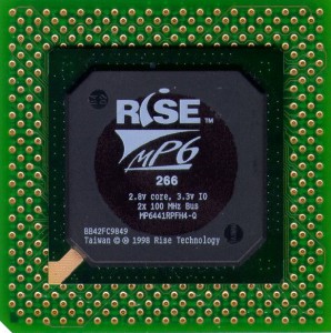
Back in 1998 a fabless CPU company introduced the Rise mP6 x86 CPU running at 166MHz Later versions ran at up to 233MHz and were Performance Rated at a somewhat generous PR300.  Rise was a bit late to the party of desktop x86 designs, and had somewhat lackluster performance.  In the 90s they had to compete with Intel, AMD, IDT, and IBM/Cyrix.  VIA, who later bought IDTs Centaur (Winchip) division, as well as Cyrix from National Semiconductor was an investor in Rise, as they were wanting an entry into the CPU market as well.  The mP6 used 16K of L1 cache and an 8 stage pipeline capable of executing 3 integer instructions per clock cycle.  This at a time when most CPUs had 32K or even 64K of L1 cache, and better branch prediction crippled the mP6.  It was used in set-top boxes and other low power type applications.  Rise licensed the core to ST Microelectronics who used it in set-top SoCs.

1998 Production Rise mP6 200MHz

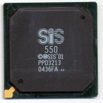
By 1999 Rise was losing money and losing sales.  In most areas this would have been the end, Rise would be a foot note in history (a smaller one then they are).  However SiS, known for their value chipsets and budget graphics cores, bought what remained of Rise and the mP6 core.  SiS wanted to develop an embedded CPU out of the mP6, and having a lack of experience took a while to make it happen.  In late 2001 they had what they wanted. The SiS 550 was at its core a 200MHz mP6 but now integrated audio, video and IDE controller all at 2/3 the power requirements of the original.

2004 Production 200MHz SiS550 CPU

The SiS550 found a home in several Thin Clients made by Neoware as well as various internet appliances.
We wrote about the SiS550 series many years ago here.

DM&P (aka Jan Yin Chan Electronics) eventually took over the design from SiS.  It is DM&P who took the lowly mP6 design into the powerful embedded CPU it is today.  The pipeline was reduced to 6 stages, and onboard 256k L2 cache was added.  The L1 cache was doubled to 32K, and the clock speed was increased to a rather quick 1GHz.

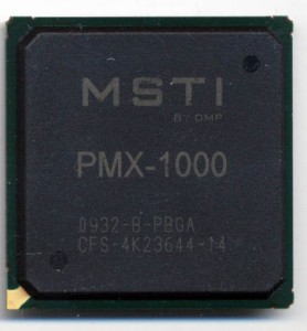
The Vortex86DX is a fully capable x86 processor.  It is perfect for very small PC applications and embedded designs where x86 code is required.  The PMX-1000 can run at up to 1GHz and adds IDE support, graphics, and HD-Audio (much like the original SiS550.

1GHz PMX-1000 - 2009

While technically an embedded CPU the PMX-1000 is fully capable of running Windows and other x86 programs.  eBox (part of DM&P) makes many small form factor, fanless, and sealed PCs based on it. It runs on a rather small 2.2Watts at 800MHz, a third the power, and 4 times the speed of the original Rise mP6.

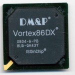
DM&P Vortex86DX

Processor Date MHz Pipelines L1 L2 Process Watts
mP6 1998 200 8 16K 0.25u 7
SiS 550

Vortex86

2001 200 8 16K 0.18u 4
Vortex86SX 2007 300 6 32K 0.13u 1
Vortex86DX

Vortex86MX

2008 1000 6 32K 256K 0.09u 2

The original Rise mP6 design is going on 12 years old and is still in wide use.  While most CPUs have switched to a RISC like design internally. the mP6, and its Vortex86 variants retain the in-order CISC architecture of the 1990’s, and for what it does, thats just fine.  Thanks to DMP Electronics for donating the Vortex86DX and PMX-1000!

Tags:
, ,

Posted in:
Research

September 23rd, 2010 ~ by admin

Arithmetic Processors: Then and Now

In the beginning there was the microprocessor.  A collection of logic that centered around an ALU (Arithmetic and Logic Unit) and a series of registers.  It was capable of doing most tasks just fine.  Simple math, and boolean logic were the key to most programming needs.  As the life of the processor and its extension, the microcontroller, progressed the computing needs became larger.  Programmers wanted to be able to manipulate larger numbers, and floating point ones at that.  Add and Subtract were no longer sufficient, division, multiplication and a host of other mathematical functions were needed.  In the 1970’s transistor counts were in the thousands, frequency in the MHz and line widths were measured in microns.  It was not feasible to build these math functions, in hardware, on the same chip (or rather die) as the processor.

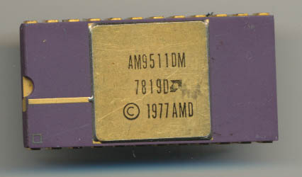
AMD AM9511DM – 2MHz Military Temp Range APU – 1978

Several companies worked to solve this.  Perhaps the most successful, and famous, was AMD.  AMD in 1977 introduced the AM9511 Arithmetic Processing Unit.  It is best described as a scientific calculator on a chip. It could handle 32 bit double precision math (via 16 bit stack/registers) and supported not just the basic ADD, SUB, MUL and DIV, but SIN, COS, TAN, ASIN, ACOS, ATAN, LOG, LN, EXP, and PWR. 14 floating point instructions, in hardware, on a single chip.  It ran at up to 3MHz (4MHz in the ‘A’ version) and could interface with pretty much any microprocessor or microcontroller, providing much needed processing power.  It was designed as a peripheral, so that the main processor could assign it a task, and then go on about its program while the AM9511 crunched the math.  The AM9511 would then notify the host processor via interrupt that it was finished the the data/status was ready to be read.

AMD updated the design to support……

Read More »

September 20th, 2010 ~ by admin

Visual Transistor-level Simulation of the 6502 CPU

Here is an interesting project.  Take very high resolution photography of a MOS 6502 die (such as that the powered the Apple 1) and use it to construct a simulater in Java that allows you to program the 6502 and watch it, on a transistor level, as it performs the program.

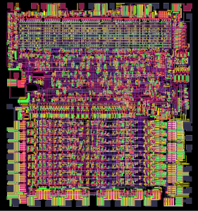
6502 Die - Visual 6502

An awesome way to see PHYSICALLY what happens for each and every instruction.  And what a great processor to do so on.  Ironically the LCD flat panel monitor you may be using? It may well be powered by a 6502 (Novatek used them in their flat panel controllers)

Check it out at Visual 6502

Tags:

Posted in:
Just For Fun, Research

September 15th, 2010 ~ by admin

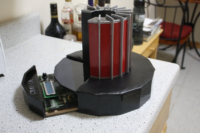
Homebrew Cray-1A – 1976 vs 2010

In 1976 the fasted normal processor ran at around 5MHz (such as the RCA 1802).  Personal computers really hadn’t been thought of, and mainframes were massive.  It was then that Seymour Cray decided to build a Super Computer. A computer that would be better and faster then most anything that existed at the time.

The Cray-1 ran at a blistering 80MHz, and could work with a staggering 32MB of memory.  This performance was not achieved in personal computers until the 1990’s.  No single processor of 1976 could attain these speeds so Cray designed his own.  Only 4 different types of ICs were used in the Cray-1 (2 types of quad-NAND gates and 2 types of SRAM)  All of the logic was ECL (Emitter Coupled Logic) which was very fast, very power hungry, and produced a lot of heat.  In all the Cray-1 used some 200,000 gates, many of which were solely used to add timing delays to make sure signaling did not generate standing waves or switching noise.

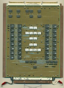
Original Cray-1 Circuit Board

Recently a man by the name of Chris Fenton decided to make a 1/10th WORKING scale model of the Cray-1A. This is no small feat, there is not a lot of surviving documentation for the Cray, nor is there much of any software left (they were mostly retired from service by 1990).  Chris wished the Cray-1 to physically look like the Original (including the padded bench seat) as well as be binary code compatible.  His implementation runs at 33MHz on a Xilinx Spartan-3E 1600 CPLD.  Basically this is a dev board with a chip that has a complex array of programmable logic that you can program to do what you want.  In this case 1.6 million gates, about 1.2 Million of which are used in the design, significantly more the the original.

Cray-1A Model

The original Cray weighed in at 5.5 tons with the cooling system, and drew around 30kW of power. The 1/10th scale? will run on a few batteries.  Supercomputers are still an important part of computing, but as vector processing expands (what the Cray was orginally diesgned for)  such things as graphics cards can be used to perform much of the tasks of a supercomputer, and do so faster and cheaper.

Regardless, when people think of a Super Computer, they think of the Cray

August 13th, 2010 ~ by admin

The evolution of the Apple iPhone and its many CPU’s – Even within a model

The CPU Shack is pretty much on the trailing edge of technology, we are, after all, a museum.  However, we fancy the new technology as well, and like to crack it open for a look see.  The iPhone, in its 4th generation, is an oasis of CPU’s, sadly we have not been able to get one.  That has now changed….

Anthony, of the iPhone repair company Milliamp.com has graciously donated the logic boards from a iPhone 2G, 3G and 3GS. No 4G iPhones yet, but perhaps later.  Now there has been several teardowns of iPhones as they came out, notably by the good folks at iFixIt.  We are going to explore the many CPUs in each model of iPhone, the changes made as they evolved, and something new though not entirely unexpected.

CPUs by function and generation of iPhone:

Function 2G 3G 3GS 4
App Processor Samsung S3C6400 400-412MHz ARM1176JZ Samsung S3C6400 400-412MHz ARM1176JZ Samsung S5PC100 600MHZ ARM Cortex A8 Apple A4 800MHz ARM Cortex A8
Baseband S-GOLD2 ARM926EJ-S <200MHz Infineon X-Gold 608 ARM926 312MHz + ARM7TDMI-S Infineon X-Gold 608 ARM926 312MHz + ARM7TDMI-S X-Gold 618 ARM1176 416MHz
GPS NA Infineon HammerHead II Infineon  HammerHead II BCM4750 (no CPU core)
Bluetooth BlueCore XA-RISC BlueCore XA-RISC BCM4325 (2 CPU cores) BCM4329 (2 CPU cores)
Wifi Marvell 88W8686 Feroceon ARMv5 128MHz Marvell 88W8686 Feroceon ARMv5 128MHz see above see above
TouchScreen Multi-chip BCM5974 TI TI
OS Nucleus by Mentor Graphics Nucleus Nucleus ThreadX by ExpressLogic
Total Cores 5 7 7 5

Applications Processor vs Baseband Processor

On a device such as the iPhone it is common to have two separate CPUs that run the phone.  The Baseband Processor runs the underlying hardware of the phone (the radios, etc)  This is critical timing wise so it runs its own OS, a Real Time OS capable of dealing with all the complexities in making a phone call or sending data to a cell tower.

The Applications Processor runs just that, the applications, such as iTunes, and iOS itself, this way they are independent of the phone portion. This way if say the new game you installed crashes, it does not effect your phone talking to the tower.

In addition to the applications processor and baseband processor there are several others.  The GPS has its own processor, as does the Bluetooth, and the Wifi as well as the touchscreen. Some of these are pretty simple CPUs, but think back  a few years.  The CPU running JUST the wifi in an iPhone is faster then most desktop computers 15 years ago.


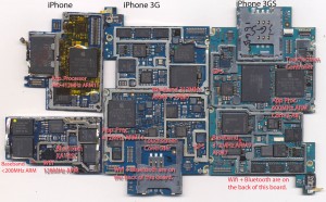
Apple iPhone Logic Boards

Apple iPhone 2G

The Original iPhone and the 3G used the same app. processor, an ARM11 based CPU made by Samsung. It initially ran at 400MHz but via a software update was bumped up to 412MHz.

The biggest change in the 2G to the 3G was the addition of GPS and a change in Baseband.  the 3Gs baseband ran at less then 200MHz, but the 3G runs at up to 312MHz, and included 2 actual ARM processors. add in the CPUs that runs the touch screen, GPS, wifi, and bluetooth and you scan see there is ALOT of processor power in the phone.  7 DIfferent CPUs just to make the phone work.

Apple iPhone 3GS

The 3GS iPhone boosted the speed of the applications processor considerably (and thus it runs iOS4 MUCH better then the 3G).  Again the app processor is made by Samsung, but now its clocked at 600MHz, and based on the ARM Cortex-A8, a faster core then the ARM11 design.  This processor will do 800+MHz but Apple underclocks it for the sake of battery life.  The baseband remains the same, but APple used an integrated chip to handle both the Bluetooth and the wifi.

Apple iPhone 4G

Previous models of iPhones carried something over from the previous model. Whether it was the app processor, baseband, or wifi, there was some reuse. Not so with the 4G, All the important bits are new.  The App processor is the same as in the iPad, the ARM Cortex-A8 based A4 (which really is a Samsung/Intrinsity design.  This design we know is capable of 1GHz (as it does such in the iPad, however, to preserve battery, its clocked at around 800MHz in the iPhone.  The Baseband processor is also all new, its now running a single ARM11 core at up to 416MHz.  The Baseband processor in the iPhone 4 is faster then the original CPU in the iPhone 3G. The Real Time OS that runs on the Baseband also changed, from Nucleos, to ThreadX. They are made by different companies (Mentor Graphics vs Express Logic) however the same designer wrote them both (William Lamie)

Apples mid-life CPU revisions

Its common for a design to evolve somewhat in the life of a product. This seems to have happened considerably within iPhone generations.

Device App Processor Part # Date Code
iPhone 339S0030 0722
iPhone 339S0042 0816
iPhone 3G 339S0036 0822
iPhone 3GS 339S0068 0919
iPhone 3GS 339S0073 0919
iPod Touch 1 339S0029 0731
iPod Touch 2 339S0048 0831
iPod Touch 3 339S0075 0928

Apple used several revisions of what SHOULD be the same CPU. the iPhone and iPhone 3G use the same processor, but here we see no less then 3 different part numbers for it.  In the 3GS we see something similar, even for devices dated the same week, there is 2 different part numbers.  Its curious what Apple/Samsung saw fit to change.  If you know of other part numbers, lets us know

Tags:
, ,

Posted in:
Research

June 8th, 2010 ~ by admin

Unlocking EPROM cores?

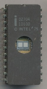
Its well known that manufacturers such as Intel and AMD will sell quad cores as dual cores, or 6-cores as quad-cores in order to meet demand, or to use dies that didn’t ‘make the cut.’ This process has been going on for over 30 years though. Back in the 70’s and 80’s it was very common for a device such as this:

Intel D2704 4k EPROM

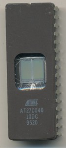
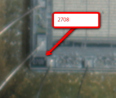
Which is a 2704 4k EPROM, to actually be made from a 2708 die, just with not all the leads connected, or sometimes, with them connected but just labeled as the smaller part. In a production environment, it is cheaper to have a single production line making dies that can be used in more then one device, then having an entire seperate production line just to make a product that may not be the most popular.  Look at this die shot (its a bit blurry) but you can see its a 2708 die.

2704 with 2708 die

Once again, whats new, really isn’t we have just went from small EPROMs, to CPUs with billions of transistors

April 9th, 2010 ~ by admin

Cyrix MediaGX: From Cyrix to AMD – A bit a History

On February 20th of 1997 Cyrix announced the MediaGX processor, running at speeds of 120 and 133MHz. By June of that year they were up to 180MHz as production was ramped at National and IBM (see press release). These processors were based on the Cyrix M1 (5×86) architecture and integrated basic graphics, and audio functions. They were sold as a ‘PC on a chip’ for budget applications, with a bit of a budget performance.

Early MediaGX Marked Gx86 120MHz circa late '96

In October 1997 Cyrix announced plans for the Cayenne cored MXi, a follow on to the MediaGX. By 1999 National Semiconductor had made some samples of it, but thats as far as it got. This was also when National Semiconductor bought Cyrix, effectively ending Intel’s lawsuit against Cyrix over x86 licensing as National held an x86 license. The Media GX was bumped to 200 and 233MHz and MMX support was added.

National Semiconductor Geode 266MHz circa 2001 Sample

Read More »