Archive for the 'Uncategorized' Category

March 23rd, 2021 ~ by admin

CPU of the Day: National Elentari x86 and What Lies Beyond – Part 2

Last week we talked about a little known, but not unheard of 486 built by National Semiconductor called the NS486 Elentari.  As interesting as a non-Intel x86 architecture is, thats not what led me down the aforementioned rabbit hole.  This is what did…

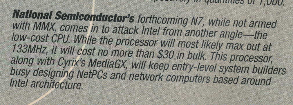
The entrance to the Rabbit hole lay in an issue of Boot Magazine.

This small blurb in Boot magazine from back in August of 1997 is all it took.  What was this mysterious N7 processor that even Boot Magazine felt the need to mention?  It is being compared to the Cyrix MediaGX, which coincidently National had agreed to merge with right about the time this issue went to press, a fact that may or may not have been known to the authors at the time.  Regardless, the deal wasn’t officially completed until 1998, so that meant this mysterious N7 had been in development for some time, and probably had reached something a bit more then a glitter in an engineers eyes….and indeed it had.

Mentions of the ‘N7’ in the press at the time start in early 1996 and continue through 1997, this indicates that the N7 was likely planned soon after the beginnings of the NS486 core.  Its very likely that the NS486 was to be a stepping stone to the bigger more powerful N7.  The N7 is described as a 133MHz ‘Pentium compatible’ processor.  The NS586 core (as it was called by National) was an enhanced NS486, with the pipeline extended to 5-stages and using Nationals new 0.35u process, just as some had originally suggested for the NS486.  This resulted in a 3.3V processor running at 133MHz.

NS586 5-Stage Pipeline – Cache could happen on Stage 3 or 4 and Memory Access was non-blocking (image (c) MPR)

The NS586 was planned to be at least 2, and most likely 3 different processors (in similar fashion to the NS486SXF and NS486SXL).  The common core to all of the designs was the 5-stage NS586.  This took the NS486 and greatly enhanced it, adding 8 of L1 cache (4K Instruction + 4K Data). The pre-fetch buffer is doubled in size to 32-bytes as well as some Out of Order execution support.  The decode and memory/cache access logic is also further optimized.  Cache accesses can be shifted between the 3rf and 4th stages as needed, allowing modifying, loading or storing of cache data in two consecutive cycles.  Unlike the K6 or PII the NS586 does not use intermediate instructions in executing x86 code, it directly executes each x86 instruction (like the NS486 before it).  The updated pipeline executes all code as fast or faster then a 486 and in some cases faster then a Pentium.  National claimed that the 133MHz core would perform as a Pentium 95, compared to say a AMD 5×86-133 being rated at a Pentium 75 level. As with the NS486 before it, it lacked an onchip FPU.

The NS586 core was not exactly small, even on the 0.35u process it took 930,000 transistors (426,000 of which is the cache).  This resulted in a die size of around 25.8mm2. (roughly the same size as the core only NS486 on 0.65u).  And it was intended to be even bigger…

Lise the NS486 before it, the NS586 was to be integrated with a variety of peripherals, and this time National was going big on the integration.   At the top was the N7-Lite, which integrated the NS586 core with a SVGA 2D graphics controller, TI TMS320C50 based DSP and Audio controller.  This in addition to a PCI bus, DMA controller USB, IrDA, and other normal peripherals of the era.  The N7-Lite does not have a traditional DRAM controller, instead using a controller geared towards a UMA (Unified Memory Architecture) to use the system RAM for the CPU and the onboard GPU. The GPU is designed to support only a TV out (NTSC PAL and SECAM outputs) as this was to be a full NetworkPC on a chip, basically what became Set-Top Boxes of the 1990’s.
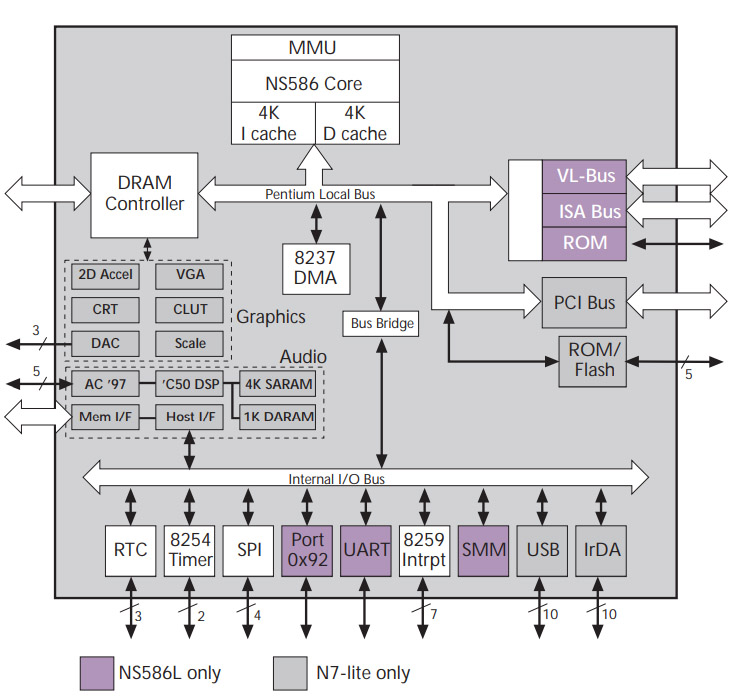
NS586L and N7-Lite shared the same core but with different peripherals as well as busses (image (c) MPR)

On the low end was the NS586L, which dropped the audio, video, and PCI bus and added a standard Pentium compatible VL-Bus, ISA, and DRAM/ROM controller, this is more of a enhanced NS486 with a similar set of peripherals, and likely would be the logical successor to designs using the 486.  Speed was to be 100MHz (again to differentiate it from the N7-Lite) and estimated cost was to be $25/chip.  Pricing for the N7-Lite was not announced. It’s unknown how far these designs progressed, whether actual silicon was made or not.  Having a transistors count and die size was indication they were pretty far along, perhaps having the chips floor plan finalized and working on taping it out for masks (6 months seems reasonable for samples after tape out).

Both of these chips were scheduled (as of October of 1997) to begin sampling in the second quarter of 1998.  Its very likely that a third chip was planned, if only due to the naming of the ‘N7-Lite.’ ‘Lite’ indicates that it is something less then the full version, and the Boot blurb (as well as some other press mentions) only refers to the ‘N7.’  In all likelihood there was to be a top end version known simply as the N7.  Such a chip would likely replace the TV only GPU in the N7-Lite with something that supports standard CRTs or LCD panels, perhaps more RAM support and Ethernet and/or an EIDE hard drive controller (something that the competing Cyrix derived ST STPC included).  We may never know, as despite the efforts of the engineering team the project was inevitably canceled in favor of the newly acquired MediaGX line from Cyrix.  This line continued to be developed at National even after they sold the rest of Cyrix off to VIA (eventually selling the MediaGX division to AMD).

Sadly they didn’t

Perhaps someone who worked in the Arador group at National can offer more insight, but until then we can only speculate of what could have been another interesting processor on the x86 scene in the 1990’s.

Posted in:
Uncategorized

February 9th, 2020 ~ by admin

ESA Solar Orbiter: When SPARCs Fly

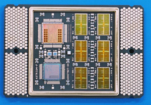
ESA ERC-32SC

ERC-32SC – SPARC V7 MCM with RAM and MIL-STD-1553

In a few hours (assuming no more delays, UPDATE: Launch Successful) the joint NASA/ESA Solar Orbiter mission will launch on a ULA Atlas 5 Rocket out of Florida, USA.  This is a mission a long time coming for the ESA, which like NASA has to get its funding from the government, except in the case of ESA, that involves the governments of many countries in the EU, which can make planning a bit more tricky.  The mission was originally baselined in 2011 and hoped to launch in…2013…then 2017..then 2018 and finally a launch date in 2020.  The original proposal dates to the late 1990’s as a mission to replace the joint NASA/ESA SOHO Solar mission that had launched in 1995.  This creates some interesting design choices for a mission, as designing often happens before a mission is completely approved/funded.  For Solar Orbiter this is one of the main reasons for it being powered by a computer that by today’s standards is rather dated, space standards no less!

Solar Orbiter – ESA

The Solar Orbiter is powered by a processor designed by the ESA, the ERC-32SC.  This is the first generation of processors designed by the ESA.  It is a SPARC V7 compliant processor running at 25MHz and capable of 20MIPS.  The ERC-32SC is a single chip version of the original ERC-32 which was a MCM (Multi chip Module) containing 3 dies that made up the processor (the Atmel/Temic TSC691 Integer Unit TSC692 FPU and TSC693 Memory Controller) that was made on a 0.8u CMOS process.  The Single chip version was made possible by a processes shrink to 0.5u.  It was also made by Atmel,  (whom acquired Temic) and is commercially known as the TSC695 as it is designed for space use, is capable of handling a 300krad Total Ionizing Dose of radiation.  The computer used in the Solar Orbiter was built by RUAG and has two seperate ERC-32SC processor systems for redundancy.  Each of the ERC-32SCs are actually mounted on a MCM, the single chip SPARC, 48MB of DRAM (38 of which is used, the remainder is for Error Detection/Correction via Reed Solomon method), and a MIL-STD-1553 bus controller/RTC/IO are included in the package.

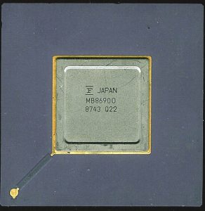
Fujitsu MB86900 – Original SPARC V7 Processor from 1987

The original specifications for this processor were developed back in the 1990’s, which is why it is a SPARC V7, equivalent to the very first Sun SPARC workstations of the late 1980’s powered by the likes of the Fujitsu MB86900/MB86901.  The ESA has developed several follow on processors since, all based on the later SPARC V8 architecture.  They are faster, and more efficient then the ERC-32SC, with some even being dual core processors.  They are known as the LEON-2 and the later LEON-3.  LEON2 has a 5-stage pipeline and no SMP support, while LEON3 increases the pipeline to 7-stages and adds SMP support.  LEON3 is also a VHDL core able to be added to many ASICS/FPGAs (LEON2 is a hard core).  The Solar Orbiter also has both LEON2 and LEON3 processors on board as well…

The Solar Orbiter caries with is 10 different scientific instruments, and each of them has their own processing subsystem, 9 of which are powered by LEON SPARC processors.  Its common for the main processor of a spacecraft to be the most powerful, but in this case the instruments each possess their own processor more powerful then that of the main spacecraft computer.   This is in large part due to many of these instruments being designed well after the original spacecraft bus and systems were baselined.  Payloads can be added/changed much later in the design of the spacecraft allowing their designers to use more modern computers.

Instrument Processor(s) Notes
Solar Orbiter OBC ERC-32SC – Atmel TSC695 Spacecraft Platform Processor
SoloHi LEON3FT – Microsemi RTAX2000 FPGA
MAG-IBS/OBS LEON3FT – Microsemi RTAX2000 FPGA
RPW-SCM/ANT LEON3FT – Microsemi RTAX4000D FPGA
LEON3FT – Cobham UT699
Two processors
SWA-HIS/EAS/PAS LEON2FT – Atmel AT697F up to 100MHz
EPD-SIS LEON2FT – IP Core
STIX LEON3FT – Microsemi RTAX2000 FPGA
EUI LEON3FT – Cobham UT699 66MHz Single core
METIS LEON2FT – Atmel AT697F
PHI LEON3FT – Cobham GR712RC Dual core up to 100MHz
SPICE 8051 + FPGA Long live the MCS-51

There is also likely more processors on this mission as well, but it can be hard to track them all down, nearly every system has its own processing (star trackers, radios/ attitude control etc)

So as you watch the launch tonight, and perhaps see science/pictures from the Solar Orbiter (or just benefit from its added help in predicting solar storms and allowing us here on Earth to prepare for them better) think of all the SPARCs it has taken to make it function.


September 5th, 2014 ~ by admin

MasPar: Massively Parallel Computers – 32 cores on a chip

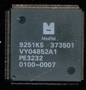
MasPar PE3232 - 32 12.5MHz 32 bit Processing Elements - 1992

MasPar PE3232 – 32 12.5MHz 32 bit Processing Elements – 1992

In the 1980’s DEC researchers were designing a supercomputer based on the Goodyear MPP from 1983.  Jeff Kalb was in charge of the division of DEC involved in this work.  The original Goodyear MPP wa based on a 1-bit processor element (PE).  DEC increased that to a 4-bit PE as well as increased the connectivity between PE’s.  When DEC decided to not commercialize the supercomputer design Kalb left (with DEC’s blessing) to start a company of his own that would.  Thus the creation of MasPar in 1987.

MasPar derives its name from the product it sought to create, a Massively Parallel supercomputer.  These type of computers, also referred to as vector processors are SIMD machines, Single Instruction, Multiple Data.  They perform the same operation on a very large set of data.  SIMD instructions are now found on most all desktop processors, where they can greatly speed up processing of multimedia.  In the late 1980’s there was several companies making such MPP computers.  Perhaps the most famous was Cray, but there was also Thinking Machine’s Connection Machine, Intel’s Paragon (i860 based), nCUBE’s hypercube, Meiko Scientific’s CS-1 (Transputer based) and several others.  Such systems cost from upwards of $100,000 each so sales were not vast, typically companies sold a few hundred to a few thousand systems.

MasPar’s first design, the MP-1 was based directly on the research done at DEC.  Each processing element contained a 4-bit ALU, a 1-bit logic unit, a 64/16 (mantissa/exponent) unit for handling floating point.  Each PE also had 48 32-bit registers.  There were designed as a 32-bit RISC processor, which means, that with the 4-bit ALU, any ALU operation would take at least 8 cycles.  This was considered acceptable in a MPP type system.  Each custom VLSI CMOS MP-1 chip contained 32 individual PE’s.  They were made on a 1.6u process and contained 400,000 transistors.  Clock speed was a fairly low 12.5MHz but this allowed the chips to be air cooled with no special cooling systems.   They were packaged in an inexpensive 208 PQFP, nothing special needed due to the low heat dissipation.  A 1024 PE board (32 chips) dissipated only 50 Watts, and an entire 16k processor system dissipated less than 1,000 watts.

Read More »

November 29th, 2010 ~ by admin

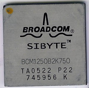
Broadcom’s MIPS Chips

A lot of talk goes on about ARM cores and their increasing use and speed.  While the market penetration, shear speed, and low power of ARM cored devices is certainly amazing its important to not forget that their are other cores in wide use as well, if not as glamorous.  The MIPS architecture was developed at around the same time as ARM (1985) and actually enjoyed success in the market much sooner then ARM did. MIPS continues to be widely used in embedded applications (expecially the MIPS 4000 architecture).

Broadcom Sibyte BCM1250B2K750 - 750MHz dual core MIPS

Broadcom is one of the largest users and producers of MIPS cores devices.  Broadcom recently announced the BRCM5000 MIPSs CPU core. It can issue 2 instructions per cycle and at 40nm runs at at least 1.3GHz (worst case speed).  It should handily clock to 2GHz+ given good process and part selection (the core uses AVS to scale voltage internally to find the perfect voltage/speed combination on a part level basis).  Broadcom chose to not use a multi-core design as a multi-core doubles die area, almost doubles power, but in typical applications does not double performance.  Using a dual-threaded design, on a dual-issue core, does provide almost a doubling of performance, at a minimum of die area.  Die area being a huge concern when the core must be integrated into various products used for mobile devices.  The BRCM5000’s predecessor (the BRCM3000) occupies a mere 1 square mm of die space at 40nm.

Broadcom is not new to the MIPS seen, they have been using them since the 1990’s when Broadcom was founded. Since then they have continually enhanced their products, via internal development, as well as many acquisitions.  Some of the more notable MIPS acquisitions were Sibyte in 2000 who made high-end MIPS network processors and the Xilleon product line from ATI/AMD in 2008 which made Digital TV Processor chips based on the MIPS core.

Just recently Broadcom closed their purchase of Beceem, a company that makes 4G chipsets based on the MIPS core.  MIPS continues to be used not just by Broadcom. Microchip’s PIC32 line is in fact a MIPS R4K processor. Cavium Networks, RMI, Toshiba, NEC, and Sony all continue to use MIPS in a variety of products.   MIPS continues to try to penetrate the smartphone industry, and if at all possible should.  The competition would help keep new innovations coming.

Tags:
,

Posted in:
Uncategorized

October 26th, 2010 ~ by admin

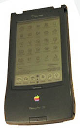
How The Newton And ARM Saved Apple From Death

Apple Newton 120 - 1994

Cult of Mac recently interviewed John Sculley, the former CEO of Apple.  The interview is long, and very interesting. Sculley presided over Apple during some rather rough times. Steve Jobs in fact still wont talk to Sculley.  This is interesting, as it was Sculley, and the result of a failure that ended up saving Apple, or at least significantly helping them stay in business.

The Apple Newton is known as one of Apple’s biggest failures, however, it ultimately brought relief to the company.  Apple began the Newton project back in 1987.  In search of a processor that could handle the OS, and run on batteries Apple turned to ARM, then a small British company known as Acorn, whose main business was computers and processors for Acorn computers and BBC Micro computers.

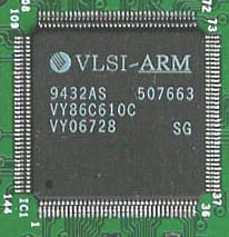
Acorn did not have the resources to design the processor Apple needed, so Apple, along with an Italian company called Olivetti took a 47% stake in Acorn.  This cash infusion allowed ARM to develop the processor for the first Newton.  The first Newtons, or MessagePads, as the ones made by Apple were branded, were powered by a 20MHz ARM610 processor.  It was made by VLSI (the first silicon partner for ARM) and called the VY86C610.  They were introduced in 1993 and continued production (in various forms) until 1997. Sharp, Motorola and several other companies also made Newton OS devices, but they enjoyed even less success then Apple’s.

VLSI VY86C610C 20MHz ARM610

In 1997 Apple releases the eMate 300, a classroom targeted laptop system.  It ran the slightly more advanced 25MHz VLSI VY86C710A ARM710A. The styling of the eMate seems to have carried over to the first iBooks with translucent, rounded cases.

The last of the line was the MessagePad 2000 and 2100, both of which were based on an ARM processor made by DEC and Intel called the StrongARM SA-110.  It ran at 162MHz and was at its time one of the highest performing designs for mobile devices available.  Intel later developed the XScale line of processors from it, which they then sold off to Marvell.

In 1998, among diminishing sales, Apple closed down the Newton division.  Some of the original developers of the Newton OS went on to create a company called Pixo.  ARM IPO’d that years as well as ARM Holdings.  Apple sold their stake in ARM for $800 Million.  This influx of cash came at a time when it was desperately needed by Apple, and gave them the time, and money they needed to ‘reset’ and return to profitability in a VERY strong way.

eMate 300 ARM710A - 25MHz

A mere 3 years later, in 2001, Apple ‘changed everything’ with the release of the iPod. The iPod ran on a dual core 90MHz ARM7TDMI processor made by PortalPlayer. It ran an OS designed by Pixo.  Apple subsequently bought Pixo, and likely returned a few old Newton employees to their old desks in doing so. All further iPods, iPhones, and iPads, and now the iTV run on ARM processors. From the lowly 20MHz of the ARM 610 to the 1GHz+ of Apple own A4. The company that Apple helped get started, is now at the foundation of Apples core business.

And it was all because of a ‘failure,’ the Newton.

Posted in:
Uncategorized

April 11th, 2010 ~ by admin

Prayers for the People of Poland

A rather large tragedy and loss. The CPU Shack sends its sympathy to the CPU collectors, and entire country of Poland for their loss. May God be with you all.

Posted in:
Uncategorized
March 6th, 2010 ~ by admin

e-readers: Making them affordable

There is no denying that e-readers are a cool piece of technology. One of the things that makes them so interesting, and popular, is the unique e-ink display. A bi-stable display that only needs power to CHANGE what it is showing. These displays use VERY little power since they only need to update content ever few minutes when say reading a book on them.

They do however require a controller to make them work, which is a seperate chip, and cost for an e-reader. A kindle, or Nook is certainly nice, but the cost is prohibitive to many.

Enter Freescale, they have developed the i.MX508 system-on-chip (SoC) combines a hardware Vizplex controller (e-ink controller) with a fast ARM Cortex-A8 applications processor and special e-reader power-savings modes.

End game? $99 E-readers, that will change the market

Source: EE Times

Posted in:
Uncategorized
February 1st, 2010 ~ by admin

The Brains of the iPad – The Apple A4 Processor

Much buzz and attention has been given to the Apple iPad, while the jury may still be out as to what Apples tablet is or isn’t useful for, one thing is true, it packs apples first self-branded processor.  Apple touted the processor of the iPad as a new creation and the most advanced yet, which is a bit of a stretch.

Apple A4

Apple A4

The Apple A4 is a ARM Cortex-A9 based SoC, it uses the ARM Mali graphics core (which is fairly robust). It was Created by P.A. Semiconductor who Apple purchased a couple years back. P.A. use to be a PowerPC company, apparently not any more. It makes sense for Apple to use an ARM based processor in the iPad as that is what powers the iPhone and iPod.  The Mali graphics core is a bit of a mystery, as Apple holds a license to its competitor, made by PowerVR, and alas the iPhone uses a PowerVR core and not a Mali core.

Essentially the Apple A4 (based on what we currently know about it) is an off the shelf design. It is not any thing revolutionary, or in fact new at all. The Nvidia Tegra 2 is also a 1GHz ARM Cortex-A9 processor. TI has a 1GHz OMAP, Qualcomm the 1GHz Snapdragon (soon to be 1.5GHz), ST has the Nomadic, and Marvel has a 1.2GHz ARM.

Perhaps then, the iPad is a ‘version 2’ product, much like the very first iPhone, Apple has lots of room to make it better, to make it outperform, and not merely match the competition. Time will tell.

UPDATE: It has been confirmed that the A4 uses PowerVR graphic (same as the iPhone) and not a Cortex-A9 but a older Cortex-A8. An even less revolutionary design. I would imagine the work APple did on the A4 involved disabling/removing various features not needed by the iPad in order to cut the power consumption even more.

Tags:
, ,

Posted in:
Uncategorized

September 6th, 2009 ~ by admin

The Renesas SuperH getts some added Super

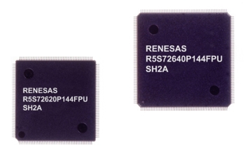
The SuperH line of microcontrollers (really full up processors now) was originally developed by Hitachi.  They have found wide use in applications spanning printer controllers to automobile control systems.  Renesas just announced yet another member of the SuperH family. The SH7264 and SH7262 both include the now common SH-2A RISC core running at 144MHz as well as a FPU, but now integrate up to 1Mbyte of SRAM on die as well as many video functions.

SuperH SH7264 and SH7262

Renesas SuperH SH7264 and SH7262

These chips can now drive displays without the need of external RAM, saving cost, and board space.  Expect to see them in such things as car navigation systems, copy machines and the like.

Source: eeProductCenter

Tags:
,

Posted in:
Uncategorized