November 22nd, 2017 ~ by admin

CPU of the Day: DEC LSI-11 Chipset

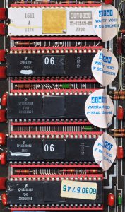
LSI-11 Chipset with EIS/FIS Chip – 1976-1977

Back in 2014 we discussed the Western Digital WD/9000 Pascal Microcomputer system.  Today we’ll look at the LSI-11 chip set, the basis of the Pascal.  Back in 1974 DEC (Digital Equipment Corporation) contracted Western Digital to design and build a 16-bit chipset to emulate the Bipolar PDP-11/05 Minicomputer.  Western Digital was paid $6.3 million for the work, and would be allowed to market and sell the resulting chipset themselves, as well as grant license to it to others (including DEC).

The LSI-11 was to be a 16-bit chipset, but was based around a 8-bit Data chips (the 1611).  The 1611 has an 8-bit ALU , 26 8-bit registers and a microinstruction register.  This is controlled by the 1621 control chip, which interprets macroinstructions from handles all the timing, as well as interrupts.  The 1621 control chip is what allows the 8-bit 1611 to be used as a 16-bit processor.  The chips are connected by an 18-bit  microinstruction bus, and a 16-bit address/data bus handles access to the rest of the system (memory/I/O).  Each microm is a 512 Word by 22-bit ROM, which can hold 80 instructions.  It is these MICROMs that allow the WD MCP1600 to function as a PDP-11/05.  The instructions in the the MICROMs (2 are required for the LSI-11) emulate the PDP-11 instructions.

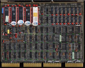
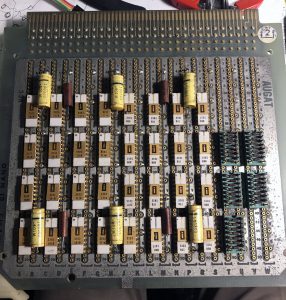
DEC M7264 LSI-11 KD11-L Board from PDP- 11/03

First production of the LSI-11 chipset began in March of 1975 with shipments commencing that year.  The PDP-11/03 based on this chipset was released later that year.  The KD-11 M7264 board formed the hear of the 11/03 (as well as other DEC systems).  In typical DEC fashion it came in many flavors with different amounts of memory, as well as different instruction support.  This was completely due to the design of the LSI-11 chipset and its MICROMs .  The basic LSI-11 needs 2 MICROMs to handle the basic PDP-11 instructions, the chipset however supported 4.  This means that more instructions could be added.  One of the most common and useful additions was the EIS/FIS (Extended Instruction Set/Floating Point Instruction Set) microm.  This added 8 more instructions including MUL, DIV, FADD, FSUB, FMUL, FDIV and 2 register shifts (ASH, ASHC).  Adding the EIS/FIS chip to a standard KD-11-F board turned it into a KD-11-L (like the one pictured).

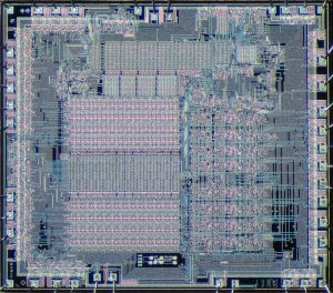
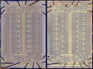
Western Digital 1611 Die –
Pauli Rautakorpi

There were other MICROMs available as well.  This included a set of 2 for support of DIBOL (Digital Business Oriented Language), a DEC language similar to COBOL.  Since the DIBOL chipset needed 2 chips a system could support DIBOL, OR EIS/FIS but not both.  MICROMs were revised as bugs were found, or faster ways of handing an instruction were made.  MICROMs revisions could also be made to support different PCB revisions.  In some ways they played the part of firmware to the PCB, as well as the instruction set for the processor.  In this way many MICROMs are specific to PCB etch revisions and other revisions of the system outside of the processor itself.  Matching the correct MICROMs, as well as Control and Data chips to the correct board is a bt of a task, and take several dozen pages of the LSI-11 maintenance manual.

Here are a few part #s to help sort things out

Data Chip
DEC 1611
Control Chip
DEC 2007C
MICROMs
MICROM 1 3010D/A
MICROM 2 3007D
EIS/FIS 3015D
Notes
21-11549-01 23-008B5-00 STD INST 1
21-15579-00 (1611H) 23-003C4-00 23-007B5-00 STD INST 2
21-16890-00 (1611H) 23-002C4-00 23-003B5-00 EIS/FIS
23-001C3 CP1621B14 23-009B5-00 EIS/FIS
23-001C2-01 CP1621B451 23-001B5-00 CP1631B103 STD INST 1
23-002B5 CP1631B073 STD INST 2
 23-091A5-01 CP1631B153 EIS/FIS
23-004B5 DIBOL 1
23-005B5 DIBOL 2
23-008A5-01 CP1631B-10 STD INST 1
23-007A5-01 CP1631B-07 STD INST 2

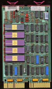
DEC M7270 LSI-11 – 1982 – All WD Chips

There are more to be found as DEC and Western Digital made many versions.  In early 1976 Western Digital licensed the MCP1600 chipset design to National Semiconductor, in exchange for some RAM technology licensing.  It is unclear if National actually made any of the MCP1600 chipset.  By 1977 DEC had started to produce the LSI-11 chip itself while continuing to source parts from Western DIgital as well.  It is common to see LSI-11 boards with DEC and WD chips mixed well into 1982.

The popularity of the PDP-11 in the 1970’s resulted in many customers for the LSI-11 based PDP’s, and their use continued well into the 1990’s with many systems continuing to be used today.  As with many such systems, they found use in industrial control and automation, where they continue to work.

November 14th, 2017 ~ by admin

CPU of the Day: Fairchild F9445: The MicroFlame Flames Out

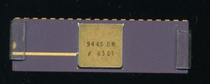
Fairchild 9445DM – 1983 Military Temp Range

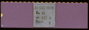
In the 1970’s many companies began to make processors based on mainframe architectures of the time. Data General with the creation of the mN601 MicroNova, TI with the TMS9900, DEC with the LSI-11 and others.  This set the stage for a pretty large showdown, as what happens when a company other then the original mainframe company creates a processor that is compatible?  This is what began to happen in the late 1970’s, and with the release of Fairchild F9440 MICROFLAME.  We’ll quote directly from the F9440 datasheet “Though structurally different from the CPUs of the Data General NOVA line of minicomputers, the 9440 offers comparable performance and executes the same instruction set.”  Specifically the bi-polar F9440 could

DGC mN602E – MicroNova – Data Generals Own single chip Nova

run most the code from the very popular Data General Nova 2 computer system.  Obviously, as Fairchild states, it is structurally different, as its Fairchilds own hardware LSI implementation.  The idea that an instruction set could be copyrighted was already being tested, and by all appearances at the time it was assumed that an Instruction set, could not be copyrighted.  This certainly helped in the wide adoption late on of x86.  A different way of protecting computer architectures had to be created then.

The first salvo was fired by Data General, in a lawsuit claiming that Fairchild’s F9440 enticed DG users to break their software license agreements.  DG’s way of ensuring they had control of their customers was to add a section in the software license agreement that the software could ONLY be ran on Data General hardware, even if it COULD run on a Fairchild F9440 (or any other hardware) it was a violation of the license to do so.  In 1978 Fairchild counter-sued, claiming that such a license was anti-competitive and seeking $10 Million in damages as a result of DG’s original suit.

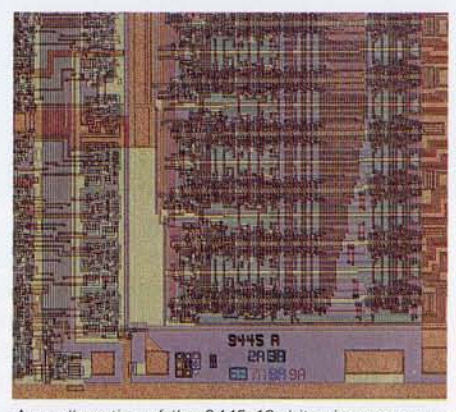
9445 DIe shot (partial)

To add fuel to the fire, Fairchild announced the F9445, the MICROFLAME II.  The F9445 was built with the same I3L (Isoplanar Integrated Injection Logic) technology but on a 2-Micron process instead of the 3-Micron process of the 9440 and contained over 5000 gates.  The F9445 could was compatible with the Nova 3 and Fairchild claimed it would be 10 times faster then the Nova 3.   The F9445 was announced in 1978 but development issues (this was one of the largest, fastest bi-polar designs) took some time and led to many delays. In 1979 Fairchild, low on cash, was purchased by  Schlumberger Limited, an oil field services company, for $425 million (Exxon responded by buying Zilog in 1980).  Production of the F9445 finally began in the first half of 1981, with deliveries beginning late in the year.  Initial devices ran at 16MHz (an increase from 12MHz in the original 9440) and 20 and 24MHz versions were released later.  The F9445 required a single +5VDC supply and a 300mA current supply dissipating about 1.5W (compared to 1W for the 9440).  The MICROFLAME II was aptly named, they ran rather hot (not unusual for their technology though). Like the F9440 the 9445 is a 16-bit processor and could directly address 128K of memory.  It adds a stack pointer and hardware multiply, while retaining the same 50 instructions from the 9440 but increases the addressing modes supported from 8 to 11 (needed to emulate the Nova 3).

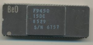
Fairchild F9450-15DC – MIL-STD-1750A processor based on the architecture of the F9445

Interestingly the F9445 provided the base for another Fairchild processor.  The F9445 took Nova instructions, decoded them and ran them on its hardware, it was, in other words, a micro-coded processor.  Microcoded processors can be useful as the microcode can be changed to support an entirely different instruction set. That’s exactly what Fairchild did with the F9450, a processor designed to execute the just released MIL-STD-1750A 16-bit instruction set.

Data General was not pleased, so again sued, claiming that Fairchild probably stole proprietary information in order to design the F9445.  Fairchild was not alone in the action as their were other companies who made Nova emulating hardware, as well as those who made software that would run on a Nova.  The lawsuits (no less then 11 of them) continued well into the 1980’s.  By 1986 Data General was struggling, the case continued, and was not going in their favor.  In September of 1986, a month before the trial for damages was to begin, Data General settled, paying Fairchild $52.5 million.  Eight years after the fireworks began, the original F9440 MICROFLAME had not been made in years, the Nova 2 and Nova 3 were no longer made as well.  The lawsuits destined the F9440 and the F9445 to failure, but they made their mark in setting precedent in lock-in, and how Instruction Sets can be used.

Read More »

October 22nd, 2017 ~ by admin

The CPU Shack Gets a Scope

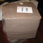
Microscope – Packed with a free roll of tape

For quite some time I have wanted a microscope for the Museum.  It would be very useful for inspecting unknown wafers and dies, as well as learning a lot more about EPROM dies.  So often one die is used for many devices, often of different sizes or even manufacturers.  Recently the Museum also received a whole bunch of MIPS prototypes, mostly all unmarked, and all with open die covers.  The only way to positively identify them, and find all the die art that the MIPS designers added, is with a scope.

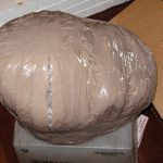
Make that 2 rolls of tape

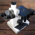
A good deal on an Accu-Ray 3035 inverted metallurgical scope showed up on eBay.  These sell new for over $2000 so at under $400 it was a good deal.  Its cost was covered by donations by many other collectors around the world, who are most likely hoping it results in more interesting article and

pretty pictures.  Metallurgical scopes are a bit different from your typical microscope.  The ‘normal’ scope is a transmitted light device, shining light THROUGH the sample into the objective.  Clearly this doesn’t work for opaque and solid items, such as wafers.  These need to use reflected light, which is a bit harder to work with.  Light is shown on the sample and reflected back into the objective.  The Accu-Ray came with 10x, 25x 40x and 60x objectives, though for wafer work 25x really is about the limit of what is needed (and it gets harder to light samples at the higher magnifica

Accu-Ray 3035 Inverted Microscope

tions).  The standard eyepieces are 10x so this results in 100x-250x magnification.  I have ordered a 4x objective and a 20x as well, which should give a good range.  The higher power

objectives have a smaller working distance, meaning they have to be much closer to the wafer/die, that can be tricky when the die is mounted in a package, or several millimeters under a window on an EPROM.

The physics of a microscope are a well understood science, getting light through the scope, to the wafer, and to the eyepiece in a way you can see anything turns out to be more of an art.  Dealing with a mirror like silicon surface, glare becomes a huge problem, so that is what I am

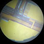
Quick shot through the eyepiece of a MIP R10000

learning about now, how to light the wafers.  The included halogen light is very nice and very bright but with wafers results in massive glare that makes seeing the wafer near impossible.  Using and LED flashlight (it bolts right up to the scope, surprisingly) results in much more even lighting, albeit less of it.  I have ordered a diffuser which should help even out the light from the halogen, hopefully that helps.

As soon as I get a good reliable set up you can look forward to some interesting pictures and hopefully some interesting new information.

Tags:

Posted in:
Museum News

October 14th, 2017 ~ by admin

VLSI: What is this THING?

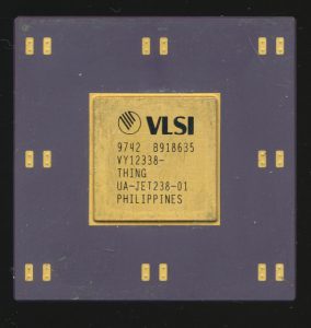
VLSI VY12338 THING UA-JET238-01 – Made in 1997

VLSI was started back in 1979 by several former Fairchild employees, 2 of which had previously founded Synertek, a connection that becomes important later on.  VLSI is best known for being a contract deign/fab services company.  They excelled at custom, and semi-custom designs for a wide range of customers, as well as acting as a foundry for customers own designs.  They became best known for their part in the development and success of the ARM processor back in the late 1980’s with ACORN.  They manufactured, as well as marketed and sold, several versions of the ARM processor, one of the few processors they actually sold themselves.  They also made a 6502 used by Apple and 65C816 (CMOS 16-bit 6502).  The 6502 was also a processor that Synertek had made back before Dan Floyd, and Gunnar Wetlesen left Synertek to start VLSI.

VLSI went on to fab processors for some of the biggest companies of the 1980’s.  The made the processor for several Honeywell BULL mainframes, built the processor for the HP A990 computer, and made dozens of chips for SGI and WANG.  VLSI also enjoyed wide success in the early 1990’s making chipsets for 486 processors, before Intel began to offer chipsets on their own in the Pentium era.

Unfortunately like LSI, most of VLSI’s designs are relatively unknown to all but them and their customer.  Marking on the chips rarely provide information on who it was made for, and even less on what exactly it does.  The above chip, marked “VY12338 THING UA-JET238-01” seems to be names as an answer to the question “What do we call this thing?”  Certainly seems to be a bit of humor on the part of some engineer.

VLSI was bought by Philips (now NXP) in 1999 so the THING may forever remain an unknown thing.

Tags:
, ,

Posted in:
Just For Fun

September 30th, 2017 ~ by admin

Processing the Page Turn

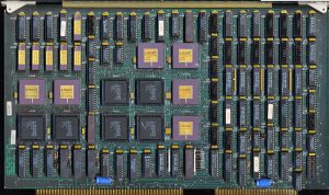
DSC Page Turn Processing Board. 6x 16bit ALUs – 1989

This board isn’t strictly a CPU but it is a processor of sorts.  I actually purchased this board as it was described as a DEC board, with not a great picture, having not seen a DEC board with LOGIC ALUs on it I bought it.  When it arrived I found it wasnt DEC at all but DSC, Digital Services Corporation.  DSC was a video effect company formed in the early 1980’s and later bought out by Chyron, one of the leaders of television video effects hardware.

In the 1980’s, effects on television were generally done in hardware, and required rather specialized hardware for each type of effect.  The most primitive were CG (Character Generators) that added captions typically to the lower third of the screen for a broadcast, like the name of the person speaking, etc.  As hardware capabilities increased, other effects could be generated, such as a video or image overlay, perspective changes or the page turn effect.

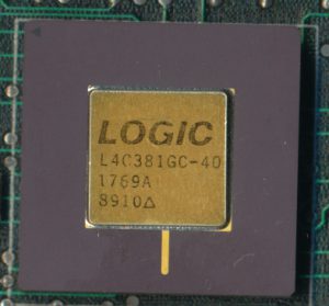
Logic L4C381GC-40 – 4x4bit ALU’s implemented in CMOS

These effects generally were handled by an effects processing system, with each effect having its own board in the system responsible for that effect.  Adding an effect required buying an effects board and installing it in the system.  This particular board from DSC handles the Page Turn Effect.  This is where one video transitions to another video with the look of a turning page.  It requires 3 inputs, the first video, the second video being turned to, and a typically solid color/image that represents the back of the page.  Here is a quick example on YouTube.  Today this can be handled by most any video editing software on a general purpose computer, but in 1989 there wasn’t a computer that could do this in near real time.

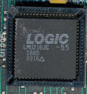
This board is built around 6 LOGIC L4C381GC-40/55 ALUs and 6x LOGIC LMU216JC-55 Multipliers.  The 4C381s are a 16-bit CMOS ALU, based on 4 74381 4-bit ALU,s a Carry Generator and interface logic.  Basically 1970’s technology updated to CMOS.  They handle 16 bit Addition, Subtraction and basic logic (XOR/OR/AND).  The LMU216s are 16 x 16-bit Parallel Multipliers.  They are the equivalent of the old AMD Am29516 that was cloned by TRW, Cypress and IDT.

LOGIC LMU216JC-55 – 16×16 CMOS Multiplier

The rest of the board consists of 6x64Kb or Video RAM, shift registers, and all the control logic (in PALs) to provide the instructions for the ALUs and multipliers.  The arrangement of the board suggests a 64-bit computation section and a 32-bit section.  Just as in the 1970’s the ALUs and multipliers have been used to make a custom processor, with a very specific instruction set and purpose and do so at a speed that would be compatible with broadcast television.  Sitting on one’s couch in the 1980’s watching TV and seeing a cool page turn effect one would think, ‘Hey that’s cool!’, yet have no idea that an entire processing system had to be designed, built and coded for that one second of television.

Russian Translation now available here by Vlad Brown

Tags:
, , ,

Posted in:
CPU of the Day

August 17th, 2017 ~ by admin

Intel Broadwell Broadens its Horizons…In Space

SpaceX CRS-12 – Carrying 116lbs of High performance Broadwell computers (image: SpaceX)

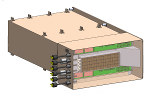
Monday’s launch of a SpaceX Falcon 9 rocket carrying a Dragon spacecraft to the space station carried what will be the most powerful computer in orbit.  In a joint project with HPE (HP Enterprise) NASA wants to test how high end computers, with off the shelf parts and construction perform in low Earth orbit.  The computer that will be soon installed is an HP Apollo 40 series (exact model is unclear, probably PC40/SX40).  It consists of 2 1U dual socket systems, running Intel Xeon E5-26xx V4 (Broadwell-EP 14nm) processors and supporting infiniband.  The only modification done was to use liquid cooling vs air cooling as the EXPRESS racks on the ISS are not set up to handle the heat load the computer generates.  The computers run on a standard 110VAC supply, provided by a NASA supplied inverter, which takes the 48VDC power generated by ISS’s solar arrays and converts it to the 110VAC needed by the Apollo computer.

The Broadwell processors are made on a 14nm process, and are some of the latest made by Intel (NASA froze the design in March so they were the fastest available to HPE at that time).  Performance will be just over 1Teraflop, a great increase over the main computers that actually RUN the ISS, which are Intel 80386SX based.  The astronauts themselves use laptops of various pedigrees, mainly Lenovo Core 2 Duo based A61Ps (these are being replaced by HP Zbook 15s powered by Intel 7th Gen Core i5 and i7 processors) , so the Apollo is a great leap up from them as well.

Mockup of HPE Apollo Computers for EXPRESS rack integrations. 2 computers with water cooling system between them.

To test the Apollo, NASA will run an identical system on the ground, performing the same tasks, and compare the outputs.  They want to see how the computers handle the environment in space, with various loads and electrical conditions.  One computer (both on the ground and on the ISS) will be run at maximum performance for the entirety of the experiment, while the other will have its computing/electrical load dynamically varied.

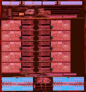
Radiation is usually one of the biggest concerns for space based computers, but on the ISS, radiation levels are not particularly high.  Daily doses experienced by the crewmembers are in the 10-50 millirad range. There are of course periods of higher radiation, either from where the ISS is in orbit, or from space weather.  The water cooling will further shield parts of the computer from radiation (water being a great radiation shield).  The Broadwell-EP processors have around 7.2 billion transistors, increasing the

10-core Broadwell die. Made on 14nm process.

chance that even a small amount of radiation may have an effect.  By running one set of computers at maximum performance, NASA can see these effects quickly.  Does the performance decrease? Does the power draw start spiking? Or is data being lost in the Infiniband networking PCIe card?

Currently experiment data has to be transferred to the ground in raw unprocessed format, as nothing on the ISS can handle the computing need to process it.  If the high performance computing experiment is successful, it can give the astronauts the ability to do processing and analysis of experimental data in orbit,. and transfer only the results to the ground, saving precious bandwidth, and allowing for experiments to be modified, changed, or created in orbit based on the ongoing results.


More Information: 

NASA: HPC COTS Experiment

HPE: The space station gets a new supercomputer

Tags:
,

Posted in:
Processor News

July 2nd, 2017 ~ by admin

ITT AN/ALQ-136 Countermeasures Processor – Bit Slice with a Bite

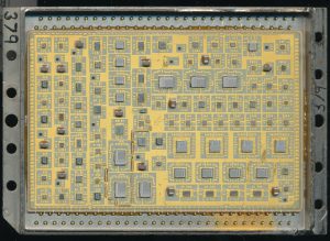
ITT 80063SM-A-919797 – AN/ALQ-136(V)I Processor. The 2901B’s are the 4 larger dies in a row, middle right.

Military computing applications require many custom designs, as they are very mission specific.  A great example is this ITT hybrid processor.  It was designed and used for the AN/ALQ-136(V)1 CMS (CounterMeasures System) for the AH-1F Cobra Attack helicopter.  Two of these hybrids are used in the system, one for the Mod Recovery board, and one for the SLO processor board.  These boards are used to detect hostile pulse RADAR systems, analyze them, and begin jamming based on what type they are.

This requires relatively fast processing, and a generally custom design.  Today a modern DSP processor could handle this task without issue.  However in the early 80’s (the AN/ALQ-136 debuted in 1982) DSP processors were in their infancy.  In 1982 a fast custom processor needed to be built with bit-slice elements.  In this case the very versatile AMD 2901 was used.  The ITT hybrid integrates 4 AMD AM2901B processor dies, as well as associated memory and interfacing elements.  The single package contains almost 100 dies, and many discrete components.  It is built on a ceramic substrate with gold traces, and sealed in a metal package.  This is required to protect the digital components of the system from electronic interference, whether from external sources, or from the helicopters own RADAR systems.  The AN/ALQ-136 is designed to prevent the Cobra from being successfully targeted by RADAR guided missiles, failure means a strong possibility that the helicopter gets hit, not something its crew would like to deal with.

4x AMD AM2901B Dies.

The 4 AMD 2901Bs run at 16MHz (50% faster then the original 2901s) and are made with ECL; together they provide 16-bit processing of the incoming RADAR signals. The SLO (Side Lobe Opposition) and MOD Recovery (Modulation Recovery) are used to determine the exact type of the enemy RADAR.  Each RADAR has a distinct characteristic that the CMS can match and respond to.  The CMS is programmed to respond to the radar signals of the most critical threat weapon systems anticipated to be encoun

Israeli AH-1F Cobras – Now Retired/Transferred to Jordan.

tered in the hostile environment.  These signatures are stored in the hybrids ROMs as well as the desired response to them.  Updates likely remain replacing these hybrids with updated versions.  New countermeasures systems (such as the 136’s replacement, the AN/ALQ-211) are more easily upgradeable to new threats.

The AH-1F Cobra continues to fly with the air forces of several countries around the world, notably Pakistan, Jordan, and Turkey.  The United States Forest Service also operates 25 AH-1F Cobras for wildland fire use, but it is rather unlikely that the countermeasures on these are operable, let alone needed.

June 20th, 2017 ~ by admin

Intel’s First: The 3101 64-bit Bipolar Memory

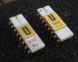
Intel 3101 Memories, from late 1969 early 1970.

Today when we think of Intel, the ‘processor company’ comes to mind.  It was now what they are best known for, but when Intel began in 1969 they did not make processors, they made memory, specifically SRAM, DRAM, and EPROMs.  The very first product Intel released, in April of 1969, was the 3101 64-bit SRAM.  It was made on the new, and fast Schottky Bipolar process.  This made it very fast (access times of 60ns) but very power hungry.  It dissipated 525mW, over half a watt, for 64-bits of memory.

Two months later Intel released the 1101, which was developed at the same time as the 3101.  It was made on a PMOS process, which allows much greater densities, the 1101 was 256-bit SRAM chip.  The sacrifice is speed, the 1101 is a bit slow, with access times of around 1.5us.  Operating power was 700mW but in standby mode it only drew 350mW.

Very Early Burroughs “D” NanoMemory board with 32 Intel 3101 memories (picture from Evan Wasserman )

Computer makers were eager for single chip memories, they allowed for more dense memory systems.  One of the first users of the 3101 was Burroughs in their ‘D’ machine, a computer designed for the Air Force in 1969.  It used 3101s for its ‘nanomemory’ organized as 64×56 bits (needing 56 3101s if they were used for all the nanomemory.  Other notable users was in implementing the stack in the Datapoint 2200.  The 2200 is the grandfather of x86, its architecture was the basis for the Intel i8008, which then led to the 8080 and 8086 processors.  The first Xerox Alto’s also used the Intel 3101, arguably the first GUI implementation.

The 3101 evolved as Intel learned the process of making chips, and assembling them.  This is notable in looking at die shots of two 3101s with lot codes likely only a few months apart.  Ken Shirriff, a fellow collector, was donated a pair of 3101s nearly identical to those pictured, for decapping and die shots, by Evan Wasserman (who donated several to the CPU Shack Museum as well).  If addition to the package difference (not the larger lid on the later one) there is some die changes as well.  The bonding pads were made much larger, likely to ease the assembly, and the main VCC line on the top of the die was made smaller.  Connections to bond pads were also cleaned up and refined.  The logic of the device appears unchanged.

3101 dies. Left is lot 898, right is the later 1116. Click for much larger version. Die photos provided by Ken Shirriff

Through the 1970’s and well into the 1980’s memory devices were by far Intel’s largest revenue source.  It wasn’t until fierce competition in the memory market that this changed.  Had it not been for IBM adopting x86, things could have been much different and more difficult for Intel.  The rapid adoption of x86 gave Intel a new revenue stream, and one that was less likely to be pressured by commodification as was happening to memory devices.


Tags:
,

Posted in:
CPU of the Day

June 5th, 2017 ~ by admin

SiFive FE310: Setting The RISC Free

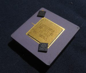
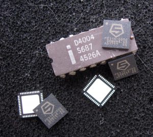
SiFive FE310 RISC-V Processor. Early LSI SPARC Processor for size comparison. Both are based on U.C. Berkeley RISC designs.

The idea of RISC (Reduced Instruction Set Computer) processors began in education, specifically University of California, Berkeley in the early 1980’s, and it was out universities that some of the most famous RISC designs came.  MIPS, still in use today, started life as a project at Stanford University, and SPARC, made famous by Sun, and now made by Oracle and Fujitsu, started life as a Berkeley University project.  Universities have continued to work with RISC architectures, for research and teaching.  The simplicity of RISC makes them an ideal educational tool for learning how computers/processors function at their basic levels.

By the late 1980’s RISC had begun to become a commercial revolution, with nearly every player having their own RISC design.  AMD (29k), Intel (i960), HP (PA-RISC), Weitek (XL8000), MIPS, SPARC, ARM, Hitachi (SH-RISC), IBM (POWER), and others offered their take on the RISC design.  Most were proprietary, while a few were licenseable, none were open architectures for anyone to use.

Unfortunately, outside of the university, RISC processors are not as simple.  The architectures, and their use may be, but licensing them for the design is not.  It can often take more time and effort to license a modern RISC processor then it does to actually implement it.  The costs to use these architectures,both in time and money often prohibit their very use.

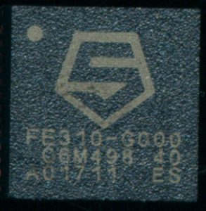
SiFive FE310 – Sample Donated by SiFive. Full 32-bit RISC on a 7.2mm2 die in a ~36mm2 package

It is out of this that SiFive began.  SiFive was founded by the creators of the first commercially successful open RISC architecture, known as RISC-V.  RISC-V was developed at Berkeley, fittingly, in 2010 and was designed to be a truly useful, general purpose RISC processor, easy to design with, easy to code for, and with enough features to be commercially useful, not limited to the classroom.  It is called the RISC-V because it is the fifth RISC design developed at Berkeley, RISC I and RISC II being designed in 1981, followed by SOAR (Smalltalk On A RISC) in 1984 and SPUR (Symbolic Processing Using RISC) in 1988.  RISC-V has already proved to be a success, it is licensed freely, and in a way (BSD license) that allows products that use it to be either open, or proprietary.  One of the more well known users is Nvidia, which announced they are replacing their own proprietary FALCON processors (used in their GPUs and Tegra processors) with RISC-V.  Samsung, Qualcomm, and others are already using RISC-V.  These cores are often so deeply embedded that their existence goes without mention, but they are there, working in the background to make whatever tech needs to work, work.

The RISC-V architecture supports 122 instructions, 98 of which are common to almost all prior RISC designs and 18 common to a few.  Six completely new instructions were added to handle unique attributes of the architecture (using a 64-bit Performance Register in a 32-bit arch.) and to support a more powerful sign-injection instruction (which can be used for absolute value, among other things). It uses 31 32-bit registers (Register 0 is reserved for holding the constant ‘0’) with optional support for 32 floating point registers.  True to the RISC design, it is a pure Load/Store processor, the only accesses to memory are via the Load/Store instructions.

Intel 4004 with 5 SiFive RISC Processors. The 4004 was meant for a calculator. The FE310 is meant for whatever your mind may dream up.

SiFive is unique among RISC IP companies.  They not only license IP but also sell processors and dev boards.  The FE310 (Freedom Everywhere 310) is a 320MHz RISC-V architecture with 16K of I-cache and 16K of scratchpad RAM fabbed by TSMC on a 180nm process. Even on this process, which is now a commodity process, the FE310’s efficient design results in a die size of only 2.65mm x 2.72mm.  On a standard 200mm wafer , this results in 3500 die per wafer, greatly helping lower the cost.  Its an impressive chip, and one that is completely open source.  What is more impressive is licensing SiFive cores, it is a simple and straightforward process.  The core (32 bit E31 or 64-bit E51) can be configured on SiFive’s site, with pricing shown as you go.  The license is a simple 7 page document that can be signed and submitted online.  Pricing starts at $275,000 and is a one time fee, there are no continuing royalty payments.  The entire process can be completed in a week or less.

In comparison, ARM, the biggest licensor of RISC processors, does not publish pricing, charges 1-2% royalties on every chip made, and has a license process that can take over a year.  The base fees start at around $1 million and go into the 10’s of millions, depending on how you want to use the IP, where it will be, and for how long.  For many small companies and users this is simply not feasible, and it is these smaller users that SiFive wishes to work with.  Licensing a processor for the next great tech, should not be the hurdle that it has become.  Many great ideas never make it to fruition due to these roadblocks.  We look forward to finding SiFive processors and cores in all sorts of products in the future.

Thanks to SiFive for their generous donation of several FE310 processors to the CPU Shack Museum.

Tags:
, , , ,

Posted in:
CPU of the Day

May 14th, 2017 ~ by admin

SESCOSEM and the French 6800

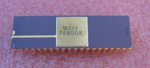
SESCOSEM SFF96800K – Dated 7651 and made by Motorola

Sescosem was a French company that was formed during the merger of Thomson-Brandt and CSF in 1968.  Thomson-Brandt has its roots as a French subsidiary of GE back in 1892 as Compagnie Française Thomson-Houston (CFTH), while CSF was a French electronics company founded in 1918.  Thomson’s SESCO division (itself a joint venture between Thomson and General Electric) was merged with CSF’s COSEM division to form SESCOSEM.  SESCOSEM made many semiconductor products for the European market, starting with basic transistors and eventually second-sourcing microprocessors.

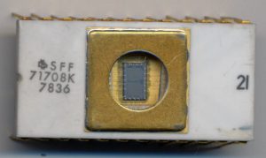
Sescosem SFF71708K – Mid 1978 – 2708 EPROM – Note the SESCOSEM logo

SESCOSEM began to work as a second-source for Motorola in September 1976.  Somewhat unusually SESCOSEM did not originally manufacture the IC’s they sold.  They received completed devices from Motorola, and remarked them as their own.  This may sound odd, but it served a purpose, it increased SESCOSEM’s market, and allowed Motorola to more easily sell their devices in Europe.  Buying local, to support the domestic industry, was, and continues to be important in Europe, so buying ‘Motorola’ devices, made in the US was less appealing then buying a ‘local’ chip, despite that chip simply being remarked. The agreement called for Motorola to supply
masks and information concerning the 6800 to Thomson-CSF (SESCOSEM parent) for present and future microprocessor products.  Eventually SESCOSEM was able to begin making their own devices at their 2 production facilities: Saint-Égrève , near Grenoble (COSEM site) and Aix-en-Provence (SESCO site).

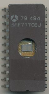
Sescosem SFF71708J – Another 2708 but made in late 1979, note the switch to the Thomson Semiconductor logo

SESCOSEM also made/sold the various support products for the 6800 series, as well as several EPROM’s, including a clone of the 1702, 2708 and 2716. In mid-1979 SESCOSEM stopped using their own logo, and switched to that of Thomson and in 1982 SESCOSEM was rolled into Thomson Semiconductor, as the French government nationalized and consolidated many industries in an attempt to increase profitability.  Thomson Semiconductor also included Mostek (sold to Thomson in 1985), Silec,  Eurotechnique (French-National Semi joint venture) and EFCIS.  This allowed Thomson to produce Motorola designs, now including the 68000 series of processors. In 1987 SGS of Italy, merged with Thomson to form SGS-Thomson, what is now known today as STMicroelectronics.

While a bit convoluted, this is one reason so many companies manufactured Motorola products.  This helped contribute to the world-wide success of Motorola products.  No longer were they only a US product, but a global product, made and sold by global companies.  In a twist of irony, Freescale, the semiconductor portion of Motorola, was purchased by NXP Semiconductors of the Netherlands in 2015, adding yet another brand of 6800 and 68000 processors.  Only a year later however, in October of 2016 Qualcomm, one of the leading makers of cell-phone chipsets, announced that it will be purchasing NXP.  A Qualcomm 68k processor may very well be in our future.