July 26th, 2015 ~ by admin

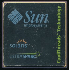
Sun CoolThreads UltraSPARC T1 Sample

Sun UltraSPARC TI Marketing Sample

Sun UltraSPARC TI Marketing Sample

The Sun UltraSPARC IV consumed 105 Watts at 1350 MHz.  This for a dual core processor that could process 2 threads.  Sun decided that the T1 (aka the Niagra) was going to change that.  It was the first ground up redesign of the SPARC core since the UltraSPARC III.  Interestingly Sun originally first attempted to develop a multithreaded process by using a pair of UltraSPARC II cores on a single die.  That project was canceled in 2004, as the T1 was in development.

The T1 was designed to focus on maximum processor utilization.  It contained up to 8 cores, each of which could process 4 threads.  This allows the processor to be used more efficiently, as a single thread can not slow down the entire processor.  All 8 cores share a single Floating Point unit.  This worked well for most database type processing, as FP instructions are not very common in that type of computing.  The T2 (made on a smaller process) allowed for a FP unit for each core which allowed better performance in HPC applications.

Made by TI on a 90nm process, the T1’s 279 million transistors consume only 72 Watts, a 30% reduction from the UltraSPARC IV at a similar clock speed.  This is what Sun called CoolThreads Technology.  Released in November of 2005 Sun was a bit ahead of their time, lower power, more efficient processors were only just beginning to become an important selling point.  Interestingly, its sister project, the UltraSPARC Rk, turned out to be not so cool.  Today, 10 years later, energy efficiency is one of the key metrics when measuring processor performance.  With data centers having on average 50,000 computers, 30 Watts per chip adds up, quick.

Tags:
,

Posted in:
CPU of the Day

July 16th, 2015 ~ by admin

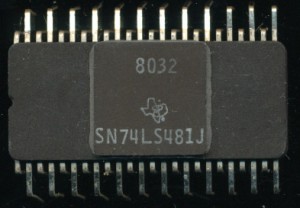
TI SN74LS481: A Better Bit-Slicer

TI SN74LS481J -1980 - 8 MHZ 4-bit Slice

TI SN74LS481J -1980 – 8 MHZ 4-bit Slice

The 1970’s was a rush to design new and innovative processors, faster, more features, and more bits.  Most of the processors were new designs, a few were single chip implementations of older mainframes (such as the TMS9900 and the Intersil 6100.  At the same time there was a competition of 4-bit processors.  Somewhat remarkable in 1976 considering 16-bit designs were now being released.  The most famous was of course the AMD AM2901, which undoubtable won the battle.  There were others, the MMI 6701 (a company which AMD would go on to merge with).  Motorola had the MC10800, made in ECL and Intel made the ill-fated (probably since it was only 2-bits) Intel 3002 Processor.  TI made the SBP0400 in I2L that enjoyed some success, but that apparently wasn’t enough.  In 1976, the same year as the SBP0400, the 6701 and the AMD AM2901, TI released the SN74S481.  This was a Schottky TTL 4-bit slice processor (and the SN74S482 sequencer for it).  It was a bit different than its competition.

Read More »

Posted in:
CPU of the Day

July 11th, 2015 ~ by admin

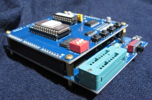
MCS-8 Test Boards Now For Sale

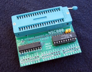
MCS-8 Test BoardThe CPU Shack Museum is pleased to announce the availability of Test Board Systems for the Intel 8008 Processor.  This system will allow you to test, as well as design program for, the Intel 8008 8-bit processor as well as its several 2nd sources, including the Siemens SAB8008, the Microsystem International MF8008 and the unlicensed East German MME U808D.

The Test System is loosely based on the 1973 MARK 8 computer, one of the very first computers to use the 8008, which was arguably the worlds first 8-bit processor.

The Boards are available here for $149 with FREE Shipping Worldwide.

Posted in:
Museum News, Products

June 27th, 2015 ~ by admin

The 16-bit Transistor level MegaProcessor

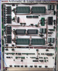
16-bit MegaProcessor ALU

16-bit MegaProcessor ALU

James Newman in Cambridge (UK) is creating a 16-bit discrete Processor Design called the Megaprocessor (there is nothing micro about it).  Not a VLSI version either, a 16-bit processor built of discrete transistors, hand wired, hand soldered, with debugging provided by…3500 LEDs.  He admits perhaps things got a bit out of hand when a co-worker remarked that it would be helpful if a signal had an LED on it, thus providing the motivation to go out and build a complete 16-bit processor.

James estimates that the design (he is still building it) will take 14,000 discrete transistors, 3,500 of which are actually to drive the LEDs.  ROM and RAM (256 bytes each, assuming he doesn’t get carpal tunnel from soldering it all) will be an extra 16,000+.

An original Intel 8086 used 29,000 transistors, and was a similar 8/16 bit architecture.  The Novix NC4016 stack processor, also 16-bits, was a very clean design using only 16,000 transistors.  HPs original BPC 16-bit processor from 1975 was 6,000, so James design is certainly inline with expectations (though his sanity maybe in question).

While this seems like a crazy amount of work (it is), This is how the first transistor computers were made.  The original DEC PDP-1 from 1959, used 2,700 discrete transistors, and was an 18-bit design.  The Apollo Guidance computer from 1966 was a 16-bit design (using IC’s with 3 transistors each, so a bit easier construction) used 12,300.

So while James’ design may be a bit over the top, it provides a good look back at where we have come.  Today chips can have well over a billion transistors on a die smaller then a fingernail.

Posted in:
Just For Fun

June 16th, 2015 ~ by admin

MCS-4/40 Test Boards once again in stock

After much delay the 4004/4040 Test Boards are now back in stock.  Only 9 of them so if you need one, order away.

Posted in:
Museum News, Products

June 11th, 2015 ~ by admin

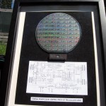
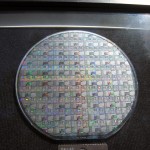
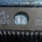
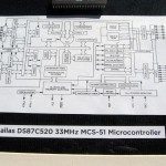
Dallas: Reaffirming the Viability of the 8-bit Processor

The introduction of the Dallas Semiconductor DS87C520 reaffirms the viability of 8-bit processors for new and demanding applications.  Those were the words written about the the Dallas DS87C520 (and its ROMLess version the DS80C320) in 1994. The Intel MCS-51 architecture it was based on had been released 13 years prior, in 1981 and ran at up to 12MHz.  By 1994 the Pentium had been released, with speeds of up to 100MHz.  Full 64-bit processors were also available, yet the 8-bit processor continued to hold on, and grow.

Dallas Semi. was founded in 1984, by former Mostek employees.  Their first products were lithium battery backed SRAMs, a product pioneered by Mostek.  Dallas added power saving and sensing circuitry to them though, greatly enhancing their usefulness.  In 1987 they combined with with an MCS-51 microcontroller to make the DS5000, which ran at 16MHz and provided battery backed SRAM.

With the release of the DS87C520 in 1994 they redesigned the MCS-51 core, allowing it to complete a machine cycle in 4-clocks vs the original 12.  They were plugin compatible, providing a simple speed up for 8051 systems.  Max clock was also raised, to 33MHz as well as additional interrupts, 16K of EPROM, an extra 1KB of SRAM and many power saving features/modes.  Other companies (such at Philips, and Atmel) began to also make enhanced 8051s, including things such as Flash memory and expanded instructions/features.

Its now 2015, and the 87C520 continues to be made, as does hundreds of other MCS-51.  It was surprising in 1994 that the 8-bit processor continued to be viable, and perhaps to some, even more so, that 21 years later, it is still viable, and shows no signs of slowing down.  The recent push into the Internet-of-Things (IoT) market has 8-bit MCUs in Internet of Things yet again.  While many companies have marked numerous 16-bit and 32-bit designs as ‘a migration path from 8-bit’, that migration is yet to be seen.  There simply is no reason, no need, and no desire to plug a 32-bit processor in where an 8-bit processor, implemented in a few thousand transistors, will do nicely.


June 2nd, 2015 ~ by admin

MG80386SX: Pin counts: How low can you go?

Intel MG80386SX16 in a 88-pin PGA

Intel MG80386SX16 in a 88-pin PGA

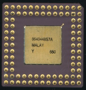
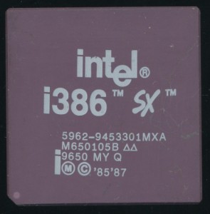
Seeing this pin out, the first processor that comes to mind probably isn’t an Intel 80386.  The 80386DX came in a 132 pin package (PGA or QFP) and the 386SX came in a 100 pin QFP.  The 386SX was the low end version of the 386.  It made do with 16 bits of Data bus, and 24 bits of Address, as opposed to the full 32-bit buses of the DX.  This accounts for 27 less pins (16 Data + 7 Address, 2 data byte selects and a 16/32 bit pin).  That covers all but 6 of the difference in package sizes.  Where are the rest from?  As with most processors, the signaling pins are not the only pins used, or not used on a package.

The 80386DX has 84 signal pins, pins that carry information to or from the processor.  It also has 40 pins for power and ground.  In the early days, when processors had only 40 pins or less, it made sense, and was feasible to have a single power and ground for the entire chip.  As complexities increased, routing became harder, and it became easier to have multiple power and ground pins to the die.  Not to mention electrically more stable, as current requirements were also increasing.  In addition the 386DX has 8 pins not used at all.  These are known as ‘No Connects.’  They are reserved for future use, or were there for testing, or simply just not needed.

Intel 5962-9453301MXA MG80386SX16 - 16MHz 80386SX - 1996 Full Milspec

Intel 5962-9453301MXA MG80386SX16 – 16MHz 80386SX – 1996 Full Milspec

Moving to the 386SX, which has 26 less signal pins (58), the standard 100 pin package used 10 No Connects and the rest (32) for power and ground.  The pictured 386SX is a late production (1996) military spec processor in an 88 pin package.  88 pins still leave plenty (30 pins) for power, ground, and no connects.  The PGA 386SX was only produced for military/industrial uses.

Why use an expensive PGA package on a low end SX processor?  The reduced bus sizes were plenty for many industrial applications while the ceramic package was much more reliable, and mechanically strong when soldered on to a board then a plastic QFP.  The PGA could work over the entire military specification, for temperature, voltage etc.  Its likely the 386SX could run on an even smaller pin count, but the PGA88 package was a standard package already in production, which often dictates how many pins a processor will have.  The same is true today, pin-count is usually driven more by what works for the package, then what the processor actually strictly needs.

Posted in:
CPU of the Day

May 20th, 2015 ~ by admin

TI TMS7000: The SCAT Microcontroller

TI TMX70P81 - Early 8K Prototype. Never released

TI TMX70P81 – Early 8K Piggyback Prototype. Never released

The 1980’s brought many 8-bit microcontrollers to the market, such famous designs as the Intel MCS-51, the Zilog Z8, and the Motorola MC680x.  There were many others as well, including TI’s entry into the market.  After the race into the market with one of the first microcomputers, the 4-bit TMS1000, and the top of the line TMS9900 16-bit processor, TI saw the need to fill in the middle, the 8-bit market.  TI didn’t want to make the 7000 series just another 8-bit MCU either, they wanted something different, not so different as to be eccentric, but something to set them apart.  They did so with an innovation they called SCAT.

TMS7000 SCAT Layout. Notice the 'strips' that form the different sections of the MCU (click to enlarge)

TMS7020 (2K EPROM + 128 bytes RAM) SCAT Layout. Notice the ‘strips’ that form the different sections of the MCU (click to enlarge)

SCAT, Strip Chip Architecture Topology, was TI’s die layout design for the TMS7000.  Instead of generating each of the blocks for the chip (SLU, ROM, RAM, etc) making them as small as possible, and then using random logic to tie them all together, they laid them out in strips on the die.  The ROM in a strip, the RAM in a strip, and the ALU etc in another.  This allowed the sections to be wired up with a minimum of random logic, resulting in a smaller die, that was also easier to test.  More importantly it allowed the TMS7000 to be easily expanded.  Adding more ROM, or RAM didn’t require redoing the entire layout, it was just added to its respective ‘strip’.

Read More »

Posted in:
CPU of the Day

May 3rd, 2015 ~ by admin

AMD AM29501: 8-bits to the ByteSlice

AMD AM29501DC - 10MHz Byte Slice

AMD AM29501DC – 10MHz Byte Slice

AMD is well known for its 2901 bit-slice processor of the 1970’s (being made well into the 1990’s), as well as the previously detailed AM29116 16-bit processor released in 1981. However, the 1980’s brought another AMD design as well, though not as complicated, it is no less interesting.  In 1981, there was not a clear DSP (Digital Signal Processor) architecture, or really purpose built design.  The Signetics 8X300 was well suited for such work, but was not inherently designed for it.  DSP tasks were handled by other processors, or by completely custom designs.  The AM29501 was not designed as a DSP, but it was marketed as a signal processor, at least for the first 5 years of manufacture.  What the 29501 was, was a relatively fast, and pipelined, byte slice processor, basically a highly upgraded AM2901.

As the name suggests, the 29501 processes data 8-bits at a time, and as a slicer, it requires external program control (it lacks a PC (Program Counter) or sequencer).  It has an 8-function ALU, and 6 sets of registers, which can be accessed independently, allowing for a pipelined architecture, multiple instructions may be issued before the first one is completed (as long as they don’t need the same resources).  While the ALU is doing some addition, more data may be fetched, or output to one of the 3 8-bit buses. AMD designed the 29501 to be able to do advanced DSP work, and such work requires multiplication, which is something the ‘501 cannot do itself.  The 29501, however, was explicitly designed to interface to the AM29516/7 16-bit multipliers.   If a multiplication is needed the microprogram controller simply puts it on the multiplier bus and tells the 2951x to handle it.  A fairly advanced system could be built by using a 29116 a 29516 as well as a 29501, building a complete pipelined DSP system.  One of the first designs using the 29501 in such a way was a finger print recognition system, for matching images of fingerprints, a particularly intense DSP task for the 1980’s.

Read More »

April 18th, 2015 ~ by admin

The Forgotten Ones: Unisys SCAMP-D Mainframe

Unisys SCAMP-D - 1997 Made by LSI

Unisys SCAMP-D – 1997 Made by LSI

Burroughs Corporation started in 1886, making it the oldest computation company still in existence.  In September 1986, Burroughs merged with Sperry Corporation (of UNIVAC fame) to form Unisys which exists to this day. The story of the SCAMP though begins in 1961, with the introduction of the Burroughs B5000 mainframe.  Burroughs was a bit late to the mainframe market, but entered it with a computer that was rather ahead of its time.  The B5000 was a stack based design, and designed from the get go with the programmer in mind, it was designed with software implementation (namely the high level languages ALGOL and COBOL) in mind, rather then wrapping software around hardware design.  This made it easy to program, and thus allowed Burroughs to take customer from IBM, who released the System/360 shortly thereafter.

In 1969 the B6500 was released, improving on the design and with it the MCP (Master Control Program).  MCP was Burroughs operating system, and what came to define their machines for the decades to come.  The B6000 line (like the B5000) was a 48-bit architecture.  In addition to the 48-bit data size was a 3-bit tag that told the system what that data was, code, data, type, etc.  This simplified the instruction set greatly as instruction need not be specific to each data type, they could check the tag and know what type of data.  Coincidentally this also allowed for greater security as well, many of the buffer overflow exploits we have seen in the modern day were not possible on a Burroughs, the tag did not allow data to be executed as code, essentially it could perform as a NX flag (No Execute) such as is on modern x86 processors.

In 1984 the first A-series was released, as well as what would become ‘e-code’ a definition of the Burroughs instruction set that could be implemented in a variety of processors.  Like the DEC VAX, Burroughs wanted to clearly define the instruction set, and leave the implementation of it up to the hardware designers.  This helped ensure robust compatibility, and future proofing, ad is why MCP programs from the 70’s still can be ran today.

Read More »

Tags:
,

Posted in:
CPU of the Day