May 20th, 2015 ~ by admin

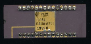
TI TMX70P81 – Early 8K Piggyback Prototype. Never released
The 1980’s brought many 8-bit microcontrollers to the market, such famous designs as the Intel MCS-51, the Zilog Z8, and the Motorola MC680x. There were many others as well, including TI’s entry into the market. After the race into the market with one of the first microcomputers, the 4-bit TMS1000, and the top of the line TMS9900 16-bit processor, TI saw the need to fill in the middle, the 8-bit market. TI didn’t want to make the 7000 series just another 8-bit MCU either, they wanted something different, not so different as to be eccentric, but something to set them apart. They did so with an innovation they called SCAT.

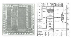
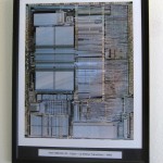
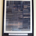
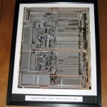
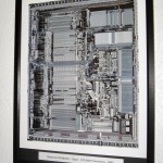
TMS7020 (2K EPROM + 128 bytes RAM) SCAT Layout. Notice the ‘strips’ that form the different sections of the MCU (click to enlarge)
SCAT, Strip Chip Architecture Topology, was TI’s die layout design for the TMS7000. Instead of generating each of the blocks for the chip (SLU, ROM, RAM, etc) making them as small as possible, and then using random logic to tie them all together, they laid them out in strips on the die. The ROM in a strip, the RAM in a strip, and the ALU etc in another. This allowed the sections to be wired up with a minimum of random logic, resulting in a smaller die, that was also easier to test. More importantly it allowed the TMS7000 to be easily expanded. Adding more ROM, or RAM didn’t require redoing the entire layout, it was just added to its respective ‘strip’.
Read More »
May 3rd, 2015 ~ by admin

AMD AM29501DC – 10MHz Byte Slice
AMD is well known for its 2901 bit-slice processor of the 1970’s (being made well into the 1990’s), as well as the previously detailed AM29116 16-bit processor released in 1981. However, the 1980’s brought another AMD design as well, though not as complicated, it is no less interesting. In 1981, there was not a clear DSP (Digital Signal Processor) architecture, or really purpose built design. The Signetics 8X300 was well suited for such work, but was not inherently designed for it. DSP tasks were handled by other processors, or by completely custom designs. The AM29501 was not designed as a DSP, but it was marketed as a signal processor, at least for the first 5 years of manufacture. What the 29501 was, was a relatively fast, and pipelined, byte slice processor, basically a highly upgraded AM2901.
As the name suggests, the 29501 processes data 8-bits at a time, and as a slicer, it requires external program control (it lacks a PC (Program Counter) or sequencer). It has an 8-function ALU, and 6 sets of registers, which can be accessed independently, allowing for a pipelined architecture, multiple instructions may be issued before the first one is completed (as long as they don’t need the same resources). While the ALU is doing some addition, more data may be fetched, or output to one of the 3 8-bit buses. AMD designed the 29501 to be able to do advanced DSP work, and such work requires multiplication, which is something the ‘501 cannot do itself. The 29501, however, was explicitly designed to interface to the AM29516/7 16-bit multipliers. If a multiplication is needed the microprogram controller simply puts it on the multiplier bus and tells the 2951x to handle it. A fairly advanced system could be built by using a 29116 a 29516 as well as a 29501, building a complete pipelined DSP system. One of the first designs using the 29501 in such a way was a finger print recognition system, for matching images of fingerprints, a particularly intense DSP task for the 1980’s.
Read More »
April 18th, 2015 ~ by admin

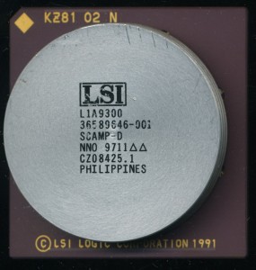
Unisys SCAMP-D – 1997 Made by LSI
Burroughs Corporation started in 1886, making it the oldest computation company still in existence. In September 1986, Burroughs merged with Sperry Corporation (of UNIVAC fame) to form Unisys which exists to this day. The story of the SCAMP though begins in 1961, with the introduction of the Burroughs B5000 mainframe. Burroughs was a bit late to the mainframe market, but entered it with a computer that was rather ahead of its time. The B5000 was a stack based design, and designed from the get go with the programmer in mind, it was designed with software implementation (namely the high level languages ALGOL and COBOL) in mind, rather then wrapping software around hardware design. This made it easy to program, and thus allowed Burroughs to take customer from IBM, who released the System/360 shortly thereafter.
In 1969 the B6500 was released, improving on the design and with it the MCP (Master Control Program). MCP was Burroughs operating system, and what came to define their machines for the decades to come. The B6000 line (like the B5000) was a 48-bit architecture. In addition to the 48-bit data size was a 3-bit tag that told the system what that data was, code, data, type, etc. This simplified the instruction set greatly as instruction need not be specific to each data type, they could check the tag and know what type of data. Coincidentally this also allowed for greater security as well, many of the buffer overflow exploits we have seen in the modern day were not possible on a Burroughs, the tag did not allow data to be executed as code, essentially it could perform as a NX flag (No Execute) such as is on modern x86 processors.
In 1984 the first A-series was released, as well as what would become ‘e-code’ a definition of the Burroughs instruction set that could be implemented in a variety of processors. Like the DEC VAX, Burroughs wanted to clearly define the instruction set, and leave the implementation of it up to the hardware designers. This helped ensure robust compatibility, and future proofing, ad is why MCP programs from the 70’s still can be ran today.
Read More »
April 12th, 2015 ~ by admin

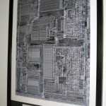
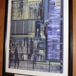
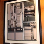
Christoph Morlinghaus in front of the very large prints of an Intel 486DX and Motorola 68030
I recently had the pleasure of helping noted photographer Christoph Morlinghaus with a die photo project. Christoph takes photos with a large format 8×10 film camera, and wanted to do some of processor dies, so the museum sent him off a box of chips. After a lot of work decapping and cleaning the chips, as well as finding ones with the most interesting dies, Christoph was able to take some stunning shots, no easy feat with the long exposure times required for such a camera. Exposure times for these shots can run into the minutes, and even something as minor as a truck driving by can create enough vibration to ruin the shot. Dies also had to be selected to show a variety of detail, colors, and be big enough to take a picture of, ideally a half inch on a side or better. You can view the results here on Morlinghaus.com. Some very large format prints are currently on display at the Snap! Gallery in Orlando Florida as well.
-

-
Intel i80186 – 1.5u – 55,000 Transistors – 1982
-

-
Intel i486 DX-33 – 1.0u – 1.2 Million Transistors – 1990
-

-
Intel Pentium 120 P54CS – 350nm – 3.3 Million Transistors – 1995
-

-
Motorola MC68020 – 2.25u – 190,000 Transistors – 1982
-

-
Motorola MC68030 – 1.0u – 273,000 Transistors – 1987
-

-
Cyrix MediaGX GXm-200GP – 350nm – 2.4 Million Transistors – 1997
-

-
Cyrix Cx486DX2-V66GP – 650nm – 1.1 Million Transistors – 1994
Christoph did 7 total die shots of a variety of processors spanning 15 years of computing. Dies included are: Intel 186, 486 and Pentium (P54CS), Motorola MC68020 and MC68030 as well as a Cyrix Media GXm and Cx486DX2. A 17″x22″print of each was donated to the CPU Shack, which are now framed and hanging, where they make a very nice display, as well as truly artistic pieces.
April 9th, 2015 ~ by admin

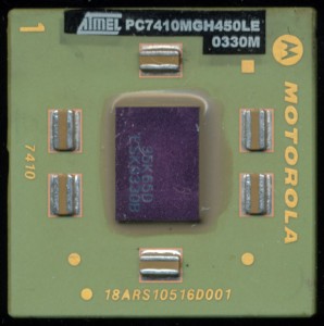
Atmel PC7410MGH450LE – Motorola Marked Package – 2003
In the 1970’s second sources were quite important in the processor industry. They provided a stable supply of a designed in part if the primary manufacturer (which often only had a fab or 2) had problems. They also could widen the market for the processor. Many of these agreements were kept active for decades after, resulting in some interesting results.
Motorola licensed many of their design to SGS, which later merged with Thomson to become STMicroelectronics. though the Thomson name was still used. Thomson license built most of Motorola’s product line, as well as many high reliability versions. In 1999 Atmel bought Thomson-CSF Semiconductors, and continued to make Motorola products (in their Grenoble France fab), which now included Motorola’s PowerPC line as well as the 68k line of processors. This portion of Atmel was sold to e2v (in England) in 2006, which continued to produce the Motorola (now spun off as Freescale) PowerPC line, now branded as e2V.
The packaging used by e2v (and previously Atmel) is the same as that used by Motorola/Freescale. The packages were custom made for Motorola/Freescale by Kyocera (and others) and so often chips with both Atmel/Motorola and e2v/Freescale markings can be found. It is this packaging that is of interest, as it shows an interesting aspect of processor design.
Read More »
March 29th, 2015 ~ by admin
Chip that come into the museum are all scanned on a Canon 5600F flatbed scanner. It has a good (there is some better though) depth of field, and its fast. Typically chips are scanned at 300dpi, or for small ones (or ones that have a die visible) 600dpi. This keep the file sizes reasonable, yet still allows them to be studied in good detail on CPUShack.com as well our records.
There are on occasion chips that are VERY hard to scan, either the markings are very small, or very shallow. This is becoming common on more modern chips, for one the chips themselves are smaller, and second, they are most often laser marked, and there isn’t enough thickness in the package (or die on some) for the Grand Canyon engraving of the 80’s.

1200 dpi dry scan
This is a Intel QG80331M500 IO Processor made by Intel in 2007. It is the replacement for the 80960 based I/O processors, using instead a 500 MHz XScale ARM Processor core. This scan was done at 1200 dpi, the part number is visible, barely, but the S-spec and FPO (lot code) are not. The markings are laser etched directly onto the surface of the silicon die. This is fairly common on this type of chip (as well as most all of Intel chipsets). How do we improve upon this? Bumping the resolution to 2400dpi just makes a bigger blurry picture (with more noise). What we need is better resolution, at where the scanner works best (less noise at 1200 dpi scan).
Thankfully we can use a ‘technology’ that is very much similar to how modern processors themselves are now made. Dumping water on the scanner, also known as immersion scanning.
Read More »
March 17th, 2015 ~ by admin

MCS-4 Test Boards
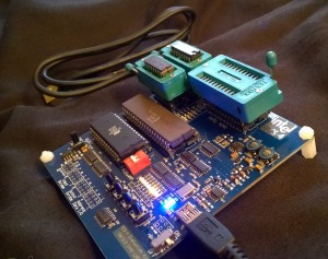
The MCS-4/40 Test boards are now back in stock and shipping this week. Only have a few available so head on over to the MCS-4 page to order yours.
I also added a PDF of the boards schematic to make interfacing to it easier for any projects you may have in mind.
If you do have a project in mind, or already made one, post about it in the comments, we’d love to see/hear about it.
March 11th, 2015 ~ by admin
Pagetable.com has in interesting post about emulators, specifically one created in 1978 to run Intel 8080 code on a 6502. While emulators today are fairly common, such as running Nintendo (6502) games on a PC, or In Circuit Emulators for development, an 8-bit cross architecture emulator is certainly different. Especially since the 8080 and 6502 were so vastly differing. Certainly a useful tool for teaching oneself a new architecture, and as they were coming out rather rapidly in the 1970’s knowing more then one was a worthy investment.
Todays equivalent perhaps would be emulating a PIC on a 8051. Perhaps someone will give it a try?
March 6th, 2015 ~ by admin

Dawn’s mission: Ceres
Dawn was launched in 2007 by NASA/JPL and was built by Orbital Sciences becoming their first interplanetary spacecraft. Dawns mission was to visit the two largest dwarf planets in the Asteroid belt, Vesta and Ceres. After visiting Vesta for over a year in 2011-2012 Dawn used its ion engines to break orbit, and travel to Ceres, a journey of 2.5 years.
In the next few hours Dawn will be captured by Ceres gravity and begin orbiting it. These protoplanets, are very interesting scientifically as they provide a look into our solar systems past. Dawn will orbit Ceres for several years and perhaps discover what the mysterious bright spots are, among other things. Studying a planet, even a dwarf planet, requires processing power, and for that Dawn is well equipped.
Dawn is solar powered, so power budgets are of great concern. At 3AU (three times further from the sun then Earth) Dawns solar panels are rates at about 1300 Watts. This has to run all the science experiments, the main computers, the comms, and most importantly the electric ion engine, which uses electricity generated from the panels to excite and eject Xenon gas at very high velocities. Thus, power consumption is more important then raw processor power here, especially for the systems that are on most of the time.
Read More »
March 1st, 2015 ~ by admin

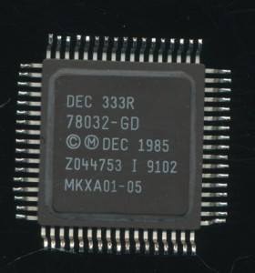
DEC 78032 DC333R MicroVAX II – 5MHz
DEC’s 32-bit VAX architecture saw many implementations since its introduction in 1977. Early implementations were all multi-chip, but as technology improved the VAX architecture could be implemented (at least partially) on a single VLSI chip. The first implementation on a single chip was the MicroVAX II released in 1985. It contained 125,000 transistors, made on a 3 micron NMOS (DEC proprietary ‘ZMOS’) process and ran at 5MHz (200ns cycle time).
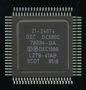
In 1987 DEC released the CVAX, the second generation VAX on VLSI. The CVAX was made on DEC’s first CMOS process, a 2 micron design using 175,000 transistors and clocked from 10-12.5 MHz (80-10ns cycle time). The input clock was a four-phase overlapping clock (so input frequency was 4x the cycle time, or 40-50MHz). Performance was 2.5-3 times better then the MicroVAX II. About half the gain was from process improvement (increased clock speed), while the rest was from architectural changes (mainly pipelining).

DEC DC580C 78034 CVAX+ 16.67MHz
As the CVAX (and its successor the CVAX+) were released the next generation was already being designed by DEC. This was to be Rigel. Rigel has a 6-stage pipeline, and was made on a 2 micron CMOS process and the CPU contained 320,000 transistors, 140k of which were for logic, while the remaining 180k were for memory (cache). The separate FPU chip contained an additional 135,000 transistors. After some early teething pains on the new CMOS process, where yields were almost non-existent, the process finally was refined enough to make commercial samples by late 1988. The target speed for Rigel was a 40ns cycle (25 MHz clock). This would give the Rigel a 6-8x performance gain over CVAX. 2X of this was from the process shrink (and doubling of clock speed) while 3X was from the improved pipelining. The remainder was due to increased memory performance, not the least of which was due to Rigels 2KB of on chip cache.
Rigel, however, had other plans…
Read More »
