February 5th, 2015 ~ by admin

TI TMS9900/SBP9900: Accidental Success

TI TMS9900JL - 1978

TI TMS9900JL – 1978

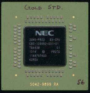
In June 1976 TI released the TMS9900 16-bit processor.  This was one of the very first 16-bit single chip processor designs, though it took a while to catch on.  This is no fault of its own, but rather TI’s failure to market it as such.  The 9900 is a single chip implementation of the TI 990 series mini-computers.  It was meant to be a low end product and thus was not particularly well supported by TI, who did not want to cut into the higher margins of their mini-computer line.    By the late 1970’s TI began to see the possibilities of the 9900 as a general purpose processor and began supporting it with development systems, support chips, and better documentation.  If TI had marketed and supported the 9900 from its release the microprocessor market very much may have turned out a bit different.  A large portion of Intel’s success (with the 808x) was not due to a good design, but rather good support and availability.

The original TMS9900 was a 3100 gate (approx 8000 transistors) NMOS design running at up to 3MHz.  It required a 4-phase clock and 3 power supplies (5V, 12V, -5V).  It had a very orthogonal instruction set that was very memory focused, making it rather easy to program.  General purpose registers were stored off chip, with only a PC, Workspace Register (which pointed to wherever the general registers would be) and a Status Register on chip.  This made context switching fairly quick and easy.  A context switch required saving only 2-3 registers. The 9900 was packaged in a, then uncommon, and expensive, 64 pin DIP.  This allowed the full 15-bits of address and 16-bits of data bus to be available.

TI had a trick up their sleeve for the 9900 line…

Read More »

Posted in:
CPU of the Day

January 27th, 2015 ~ by admin

MCS-4 Test Boards now available for Sale

MCS-4 Test Boards

MCS-4 Test Boards

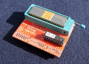
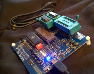
The CPU Shack is excited to now offer MCS-4 test boards for sale and shipping now. These boards are intended to test Intel 4004 and 4040 processors as well as 4002 RAMs.  They can also test National Semiconductor 4004s and 4002s.

Each board runs off of a min-USB connector making it very easy to use. The processors are inserted into easy to use ZIF sockets making testing many different CPUs a snap. I

Head on over to the MCS-4 page to buy yours today!

Posted in:
Products

January 18th, 2015 ~ by admin

Hua Ko HKE65SC02PL – GTE Micros Asian Twin

Hua Ko CMOS 6502 - 4Mhz Industrial Temp - Direct copy from GTE Micro

Hua Ko CMOS 6502 – 4Mhz Industrial Temp – Direct copy from GTE Micro

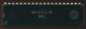
Hua Ko Electronics was started in 1979 in Hong Kong, though with close ties to the PRC. Their story is a bit more interesting then their products, which were largely second sources of western designs. In 1980 they started a subsidiary in San Jose, CA. This was a design services center mainly ran as a foundry for other companies. They developed mask sets in their CA facility but wafer fab and most assembly was done back in Hong Kong (as well as the Philippines by 1984). Chipex also had a side business, they were illegally copying clients designs and sending them back to the PRC. In addition they were sending proprietary (and restricted) equipment back to Hong Kong and the PRC. in 1982 their San Jose facilities were raided and equipment seized. Several employees were arrested and later charged and convicted. The following investigation showed that the PRC consulate had provided support and guidance for Chipex’s operations and illegal activities. So where exactly did the HKE65SC02 design come from?

Read More »

January 16th, 2015 ~ by admin

Sun UltraSPARC Rock: When is a core not a core?

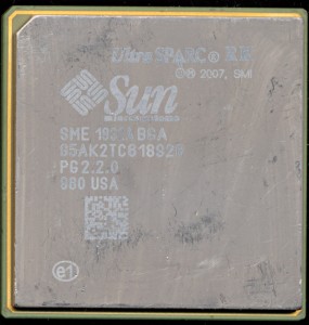
Sun SME1832ABGA PG 2.2.0 UltraSPARC RK - 2007 Sample

Sun SME1832ABGA PG 2.2.0 UltraSPARC RK – 2007 Sample

In 2005 Sun (now Oracle) began work on a new UltraSPARC, the Rock, or RK for short.  The RK was to introduce several innovative technologies to the SPARC line and would complement the also in development (and still used) T-series.  The RK was to support transactional memory, which is a way of handling memory access that more closely resembles database usage (important in the database server market).  Greatly simplified, it allows the processor to hold or buffer multiple instruction results (load/stores) as a group, and then write the entire batch to memory once all had finished.  The group is a transaction, and thus the result of that transaction is stored atomically, as if it were the result of a single instruction.

The RK also was designed as a 16-core processor, with 4 sets of cores forming a cluster.  This is where the definition of a core becomes a source of much debate.  Each 4-core cluster shared a single 32KB Instruction cache, a pair of 32KB Data caches, and 2 floating point units (one of which only handled multiplies).  This type of arrangement is often called Clustered Multi-threading.  Since floating point instructions are not all the common in a database system, it made sense to share the FPU resources amongst multiple ‘cores.’

The RK was designed for a 65nm process with a target frequency of 2.3GHz, while consuming a rather incredible 250W (more power than an entire PC drew on average at the time).
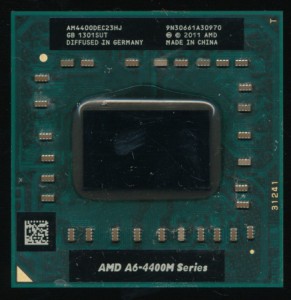
AMD A6-4400M - 2 'cores' with shared FPU and cache.

AMD A6-4400M – 2 ‘cores’ with shared FPU and cache – Piledriver Architecture

This should sound familiar, as its also the basis of the AMD Bulldozer (and later) cores released in 2011.  AMD refers to them as Modules rather then clusters, but the principle is the same.  a Module has 2 integer units, each with their own 16K data cache.  a 64K instruction cache and a single floating point unit is shared between the two.  The third generation (Steamroller) added a second instruction decoder to each module.

The idea of CMT, however, is not new, its roots go all the way back to the Alpha 21264 in 1996, nearly 10 years before the RK.  The 21164 had 2 integer ALUs and an FPU (the FPU was technically 2 FPUs, though one only handled FMUL, while the other handled the rest of the FPU instructions) .  The integer ALUs each had their own register file and address ALU and each was referred to as a cluster.  Today the DEC 21264 could very well have been marketed as a dual core processor.

The SPARC RK turned out to be better on paper then in silicon.  In 2009 Oracle purchased Sun and in 2010 the RK was canceled by Larry Ellison.  Larry Ellison, never one to mince his words said of the RK:  “This processor had two incredible virtues: It was incredibly slow and it consumed vast amounts of energy. It was so hot that they had to put about 12 inches of cooling fans on top of it to cool the processor. It was just madness to continue that project.”  While the Rock (lava rock perhaps?) never made it to market, samples were made and tested, and a great deal was learned from it.  Certainly experience that made its way into Oracle’s other T-Series processors.

December 20th, 2014 ~ by admin

Monsanto: Bringers of the Light

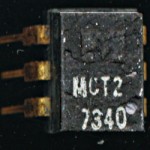
Monsanto MCT2 - LED Based Opto-coupler

Monsanto MCT2 – LED Based Opto-coupler

This little chip, dated from 1973, is part of the history of what we are surrounded by, LEDs.  And they have an unlikely and somewhat surprising beginning.  The MCT2 is an opto-coupler, basically an LED and a phototransistor in a single package, used for isolating digital signals.  The important portion here is the LED.  LEDs are in nearly every electronic product these days, and this Christmas season we see many Christmas lights that are now LED based.  THey are more efficient, and much longer lasting.  Certainly the eco-friendly choice for lighting.  And they have their roots in a company that does not always elicit an eco-friendly discussion.

That would be Monsanto.

That big ‘M’ on the package is for Monsanto, who from 1968-1979 was the leading supplier of LEDs and opto-electronics.  In 1968 there were exactly 2 companies who made visible light LEDs (red), HP and Monsanto, and HP used materials supplied by Monsanto to make theirs.

LED Christmas Lights

Read More »

December 13th, 2014 ~ by admin

TriMedia TM-1300: VLIW Processor for the World

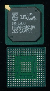
TiMedia TM-1300 - Marketing Sample

TiMedia TM-1300 – Marketing Sample

The roots of TriMedia start in 1987 at Philips with Gerrit Slavenburg (who wrote actual forwards for most of the Datasheets) and Junien Labrousse as the LIFE-1 processor.  At its heart it was a 32-bit VLIW (Very Long Instruction Word) processor. VLIW was a rather new concept in the 1980’s, and really didn’t catch on until the late 90’s.  Intel’s i860 could run in superscalar, or VLIW mode in 1989 but ended up a bit of a flop.  TI made the C6000 lince of the TMS320 DSP which was VLIW based.  By far thos most famous, or perhaps infamous, VLIW implementation were the Transmeta, and the Itanium, both of which proved to be less then successful in the long run (though both ended up finding niche markets).

TriMedia, released their first commercial VLIW product in 1997, the TM1000.  As the name suggests, TriMedia Processors are media focused.  They are based around a general purpose VLIW CPU core, but add audio, video and graphics processing.  THe core is decidedly not designed as a standalone processor.  It implements most CPU functions but not all, for example, it supports only 32-bit floating point math (rather than full 64 or 80 bit).

The TM-1300 was released in 1999 and featured a clock speed of 166MHz @ 2.0V on a 0.25u process.  At 166MHz the TM-1300 consumed about 3.5W, which at the time was relatively low.  It had 32K of Instruction Cache and 16K of Data Cache. As is typical of RISC processors the 1300 had 128 general purpose 32-bit registers. The VLIW instruction length allows five simultaneous operations to be issued every clock cycle. These operations can target any five of the 27 functional units in the processor, including integer and floating-point arithmetic units and SIMD units.

The above picture TM-1300 was a marketing sample handed out to the media during the Consumer Electronics Show for the processors release in 1999.  It is marked with the base specs of the chip as well as CES SAMPLE.  Likely these were pre-production units that didn’t meet spec or failed inspection, remarked for media give-aways.

Read More »

Posted in:
CPU of the Day

December 8th, 2014 ~ by admin

Makings of a Comet: The VAX 11/750

DEC 608B 19-14682-00 VAX750 ALP - 4- bit slice

DEC 608B 19-14682-00 VAX750 ALP – 4- bit slice

In the mid-1970’s DEC saw the need for a 32-bit successor to the very popular PDP-11.  They developed the VAX (Virtual Address eXtension) as its replacement.  Its important to realize that VAX was an architecture first, and not designed from the beginning with a particular technological implementation in mind.   This varies considerably from the x86 architecture which initially was designed for the 8086 processor, with its specific technology (NMOS, 40 DIP, etc) in mind.  VAX was and is implemented (or emulated as DEC often called it) in many ways, on many technologies.  The architecture was largely designed to be programmer centric, writing software for VAX was mean to be rather independent of what it ran on (very much like what x86 has become today).

The first implementation was the VAX 11/780 Star, released in 1977, which was implemented in TTL, and clocked at 5MHz.  TTL allowed for higher performance, but at the expense of greater board real estate as well as somewhat less reliability (more IC’s means more failure points). It also cost more, to purchase, to run, and to cool.

DEC followed the Star with the 11/750 Comet in 1980.  This was a value version of the Star.  It ran at only 3.12MHz (320ns cycle time) but introduced some new technology.  Part of the ‘value’ was a much smaller footprint.  The TTL had been replaced by bi-polar gate arrays.  Over 90% of the VAX architecture was implemented in the gate arrays, and there was a lot of them, 95 in a complete system with the floating point accelerator (28 arrays).  The CPU and Memory controller used 55 while the Massbus (I/O) used an additional 12 gate arrays.  The 95 gate arrays though replaced hundreds of discrete TTL chips.  And as a further simplification they were all the same gate array.

Read More »

Tags:
,

Posted in:
CPU of the Day

November 25th, 2014 ~ by admin

MCS-80 Test Boards For Sale at the CPU Shack

MCS-80 testboard with included Tungsram 8080APC processor

MCS-80 testboard with included Tungsram 8080APC processor

The CPU Shack is excited to now offer MCS-80 test boards for sale and shipping now.  These boards are intended to test Intel 8080A processors as well as their many compatible second sources and clones (such as AMD, NEC, Toshiba, and many more!

Each board runs off of a min-USB connector making it very easy to use.  The 8080 processor is inserted into an easy to use ZIF socket making testing many different CPUs a snap.  Included with each board is a working Tungsram 8080APC processor, an Intel copy made in Hungary.

Head on over to the MCS-80 page to buy yours today!

November 21st, 2014 ~ by admin

When a Minicomputer becomes a Micro: the DGC microNOVA mN601 and 602

DGC logoThe late 1960’s and early 1970’s saw the rise of the mini-computer.  These computers were mini because they no longer took up an entire room.  While not something you would stick on your desk at home, they did fit under the desk of many offices.  Typically there were built with multiple large circuit boards and their processor was implemented with many MSI (medium scale integration) IC’s and/or straight TTL.  TTL versions of the 1970’s often were designed around the 74181 4-bit ALU, from which 12, 16 or even 32-bit processor architectures could be built from.  DEC, Wang, Data General, Honeywell, HP and many others made such systems.

By the mid-1970’s the semiconductor industry had advanced enough that many of these designs could now be implemented on a few chips, instead of a few boards, so the new race to make IC versions of previous mini-computers began.  DEC implemented their PDP-11 architecture into a set of ICs known as the LSI-11. Other companies (such as GI) also made PDP-11 type IC’s.  HP made custom ICs (such as the nano-processor) for their new computers, Wang did similar as well.

Data General was not to be left out.  Data General was formed in 1968 by ex DEC employees whom tried to convince DEC of the merits of a 16-bit minicomputer.  DEC at the time made the 12-bit PDP-8, but  Edson de Castro, Henry Burkhardt III, and Richard Sogge thought 16-bits was better, and attainable.  They were joined by Herbert Richman of Fairchild Semiconductor (which will become important later on.)  The first minicomputer they made was the NOVA, which was, of course, a 16-bit design and used many MSI’s from Fairchild.  As semiconductor technology improved so did the NOVA line, getting faster, simpler and cheaper, eventually moving to mainly TTL.

Read More »

Posted in:
CPU of the Day

November 15th, 2014 ~ by admin

Apple A8X Processor: What does an X get you?

Anandtech has an excellent article on the new Apple A8X processor that powers the iPad Air 2.  This is an interesting processor for Apple, but perhaps more interesting is its use, and the reasoning for it.  Like the A5X and A6X before it (there was no A7X) it is an upgrade/enhancement from the A8 it is based on.  In the A5X the CPU was moved from a single core to a dual core and the GPU was increased from a dual core PowerVR SGX543MP2 to a quad-core PowerVR SGX543MP4.  The A6X kept the same dual core CPU design as the A6 but went from a tri-core SGX543MP3 to a quad core SGX554MP4.  Clock speeds were increased in the A5X and A6X over the A5 and A6 respectively.

The A8X continues on this track.  The A8X adds a third CPU core, and doubles the GX6450 GPU cores to 8.  This is interesting as Imagination Technologies (whom the GPUs are licensed from) doesn’t officially support or provide an octa-core GPU.  Apple;s license with Imagination clearly allows customization though.  This is similar to the ARM Architecture license that they have.  They are not restricted to off the shelf ARM, or Imagination cores, they have free reign to design/customize the CPU and GPU cores.  This type of licensing is more expensive, but it allows much greater flexibility.

This brings us to the why.  The A8X is the processor the the newly released iPad Air 2, the previous iPad air ran an A7, which wasn’t a particularly bad processor.  The iPad Air 2 has basically the same spec’s as the previous model, importantly the screen resolution is the same and no significantly processor intense features were added.

When Apple moved from the iPad 2 to the iPad (third gen) they doubled the pixel density, so it made sense for the A5X to have additional CPU and GPU cores to handle the significantly increased amount of processing for that screen. Moving from the A7 to the A8 in the iPad Air 2 would make clear sense from a battery life point of view as well, the new Air has a much smaller batter so battery life must be enhanced, which is something Apple worked very hard on with the A8.  Moving to the A8X, as well as doubling the RAM though doesn’t tell us that Apple was only concerned about battery life (though surely the A8X can turn on/off cores as needed).  Apple clearly felt that the iPad needed a significant performance boost as well, and by all reports the Air 2 is stunningly fast.

It does beg the question though? What else may Apple have in store for such a powerful SoC?