November 25th, 2014 ~ by admin

MCS-80 Test Boards For Sale at the CPU Shack

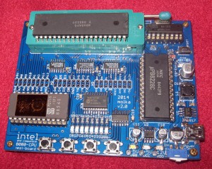
MCS-80 testboard with included Tungsram 8080APC processor

MCS-80 testboard with included Tungsram 8080APC processor

The CPU Shack is excited to now offer MCS-80 test boards for sale and shipping now.  These boards are intended to test Intel 8080A processors as well as their many compatible second sources and clones (such as AMD, NEC, Toshiba, and many more!

Each board runs off of a min-USB connector making it very easy to use.  The 8080 processor is inserted into an easy to use ZIF socket making testing many different CPUs a snap.  Included with each board is a working Tungsram 8080APC processor, an Intel copy made in Hungary.

Head on over to the MCS-80 page to buy yours today!

November 21st, 2014 ~ by admin

When a Minicomputer becomes a Micro: the DGC microNOVA mN601 and 602

DGC logoThe late 1960’s and early 1970’s saw the rise of the mini-computer.  These computers were mini because they no longer took up an entire room.  While not something you would stick on your desk at home, they did fit under the desk of many offices.  Typically there were built with multiple large circuit boards and their processor was implemented with many MSI (medium scale integration) IC’s and/or straight TTL.  TTL versions of the 1970’s often were designed around the 74181 4-bit ALU, from which 12, 16 or even 32-bit processor architectures could be built from.  DEC, Wang, Data General, Honeywell, HP and many others made such systems.

By the mid-1970’s the semiconductor industry had advanced enough that many of these designs could now be implemented on a few chips, instead of a few boards, so the new race to make IC versions of previous mini-computers began.  DEC implemented their PDP-11 architecture into a set of ICs known as the LSI-11. Other companies (such as GI) also made PDP-11 type IC’s.  HP made custom ICs (such as the nano-processor) for their new computers, Wang did similar as well.

Data General was not to be left out.  Data General was formed in 1968 by ex DEC employees whom tried to convince DEC of the merits of a 16-bit minicomputer.  DEC at the time made the 12-bit PDP-8, but  Edson de Castro, Henry Burkhardt III, and Richard Sogge thought 16-bits was better, and attainable.  They were joined by Herbert Richman of Fairchild Semiconductor (which will become important later on.)  The first minicomputer they made was the NOVA, which was, of course, a 16-bit design and used many MSI’s from Fairchild.  As semiconductor technology improved so did the NOVA line, getting faster, simpler and cheaper, eventually moving to mainly TTL.

Read More »

Posted in:
CPU of the Day

November 15th, 2014 ~ by admin

Apple A8X Processor: What does an X get you?

Anandtech has an excellent article on the new Apple A8X processor that powers the iPad Air 2.  This is an interesting processor for Apple, but perhaps more interesting is its use, and the reasoning for it.  Like the A5X and A6X before it (there was no A7X) it is an upgrade/enhancement from the A8 it is based on.  In the A5X the CPU was moved from a single core to a dual core and the GPU was increased from a dual core PowerVR SGX543MP2 to a quad-core PowerVR SGX543MP4.  The A6X kept the same dual core CPU design as the A6 but went from a tri-core SGX543MP3 to a quad core SGX554MP4.  Clock speeds were increased in the A5X and A6X over the A5 and A6 respectively.

The A8X continues on this track.  The A8X adds a third CPU core, and doubles the GX6450 GPU cores to 8.  This is interesting as Imagination Technologies (whom the GPUs are licensed from) doesn’t officially support or provide an octa-core GPU.  Apple;s license with Imagination clearly allows customization though.  This is similar to the ARM Architecture license that they have.  They are not restricted to off the shelf ARM, or Imagination cores, they have free reign to design/customize the CPU and GPU cores.  This type of licensing is more expensive, but it allows much greater flexibility.

This brings us to the why.  The A8X is the processor the the newly released iPad Air 2, the previous iPad air ran an A7, which wasn’t a particularly bad processor.  The iPad Air 2 has basically the same spec’s as the previous model, importantly the screen resolution is the same and no significantly processor intense features were added.

When Apple moved from the iPad 2 to the iPad (third gen) they doubled the pixel density, so it made sense for the A5X to have additional CPU and GPU cores to handle the significantly increased amount of processing for that screen. Moving from the A7 to the A8 in the iPad Air 2 would make clear sense from a battery life point of view as well, the new Air has a much smaller batter so battery life must be enhanced, which is something Apple worked very hard on with the A8.  Moving to the A8X, as well as doubling the RAM though doesn’t tell us that Apple was only concerned about battery life (though surely the A8X can turn on/off cores as needed).  Apple clearly felt that the iPad needed a significant performance boost as well, and by all reports the Air 2 is stunningly fast.

It does beg the question though? What else may Apple have in store for such a powerful SoC?

November 12th, 2014 ~ by admin

Here comes Philae! Powered by an RTX2010

Comet 67P/Churyumov–Gerasimenko - Soon to have a pair of Harris RTX2010 Processors

Comet 67P/Churyumov–Gerasimenko – Soon to have a pair of Harris RTX2010 Processors

In less then an hour (11/12/2014 @ approx 0835 GMT) 511,000,000 km from Earth the Philae lander of the Rosetta mission will detach and begin its decent to a comets surface.  The orbiter is powered by a 1750A processor by Dynex (as we previously discussed).  The lander is powered by two 8MHz Harris RTX2010 16-bit stack processors, again a design dating back to the 1980’s.  These are used by the Philae CDMS (COmmand and Data Management System) to control all aspects of the lander.

All lander functions have to be pre programmed and executed by the CDMS with absolute fault tolerance as communications to Earth take over 28 minutes one way.  The pair of RTX2010s run in a hot redundant set up, where one board (Data Processing Unit) runs as the primary, while the second monitors it, ready to take over if any anomaly is detected.  The backup has been well tested as on each power cycle of Philae the backup computer has started, then handed control over to the primary.  This technically is an anomaly, as the CDMS was not programmed to do so, but due to some unknown cause it is working in such a state.  The fault tolerant programming handles such a situation gracefully and it will have no effect on Philae’s mission.

Why was the RTX2010 chosen?  Simply put the RTX2010 is the lowest power budget processor available that is radiation hardened, and powerful enough to handle the complex landing procedure.  Philae runs on batteries for the first phase of its mission (later it will switch to solar/back up batteries) so the power budget is critical.  The RTX2010 is a Forth based stack processor which allows for very efficient coding, again useful for a low power budget.

Eight of the instruments are also powered by a RTX2010s, making 10 total (running at between 8-10MHz).  The lander also includes an Analog Devices ADSP-21020 and a pair of 80C3x microcontrollers as well as multiple FPGAs.


November 3rd, 2014 ~ by admin

Real3D – From Tank Simulators to Graphics Cards

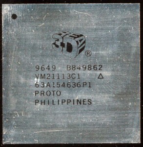
Real3D VM21113C1 Prototype (likely a Pro/1000)

Real3D VM21113C1 Prototype (likely a Pro/1000)

Much of consumer tech starts life in the labs of defense companies.  The reasons of course are simple, defense projects demand high tech, and are paid high prices by their respective governments.  Usually this tech is eventually spun off or licensed to consumer companies.  Occasionally, however, a defense company will commercialize a product on their own.  Thus was the case of Real3D.

Real3D has its roots in GE Aerospace.  GE needed to make simulators, with graphics good enough to be useful for training for a variety of systems.  Their first system was a docking simulator for the Apollo Project in the 1960’s.  By the 1980’s the technology had evolved into graphics systems for other  simulators, notably the M1 Tank.  This simulator used texture mapping graphics, which was in the world of sprites commonly used on PC’s was rather high tech. In 1992 GE sold the GE Aerospace division to Martin-Marietta who then merged with Lockheed.  Lockheed Martin wanted to commercialize the graphics work GE Aerospace has developed and thus formed Real3D Inc.  in 1995. Real3D’s first commercial success was the graphics work on the Sega Model 2 (Real3D/100) and 3 (Pro-1000) arcade systems.  Real3D also began working with SGI and Intel on a PC based graphic solution to take advantage of the new AGP bus.  This was known as the Starfighter, and later as the rather infamous Intel i740, its performance was not particularly good, but it was what Intel wanted for their entry into the value graphics market.  Real3D also had the Pro-1000 whose performance was much better but it never made it out of the development stage.

In 1999 Lockheed closed Real3D and sold its assets (mainly IP)  to Intel.  The i740 was withdrawn from the market in 1999 as well, but its technology, and that of Real3D continued to be used by Intel in their integrated graphics chipsets (notably the i810 and i815), surviving still to this day.  While no competitor to AMD/Nvidia Graphics it still is enough for most computing.

Posted in:
GPU

October 30th, 2014 ~ by admin

SGS-Ates M380 and GI LP8000 – 8 Bits for Europe

SGS-Ates M380B1 - 1977

SGS-Ates M380B1 – 1977

In the 1970’s the computer age was booming.  New processor designs were being pushed out by the month, and computers to use them were being designed and outdated just as fast.  Not all markets were growing as fast as the American market, or could support the newest, most complex, and expensive designs.  Thus, it was common for semiconductor companies to design chips specifically for these markets.  Europe was considered one of these markets, where simpler more affordable devices were easier to sell, thus CPUs were made specifically for the European market.  Many of these designs are still nearly impossible to find outside of Europe.

General Instruments was one such company.  Their premier processor, the CP1600, was a 16-bit deign based on the PDP-11.  It was one of the first NMOS 16-bit processors (along with the TI9900) and was released in 1975.  GI also had the PIC line of 8-bit MCUs for control oriented tasks, which is still in production today.  GI wanted a design for the European market so in 1976 released the LP8000, LP for Logic Processor.  The LP8000 was a 3-chip simple processor and cost a mere $10.  It could execute 48 instructions (including ADD, but subtraction was not supported directly) at a clock speed of 800 kHz and was made on a PMOS process. The chipset consisted of the LP8000 processor which contained the ALU and 48 8-bit registers as well as the accumulator a 6-bit address bus and 8-bit of I/O.  Combining the 6-bit address and 8-bit I/O busses allowed the LP8000 to directly address 16K of memory.  The 11-bit Program Counter was contained off chip, on the LP6000 which also contained an additional 16 lines of I/O and 1K of ROM for program storage.  Clock generation was provided by the LP1030 and memory expansion was handled by the LP1000 (which also includes a 11-bit PC for interfacing up to 2K of memory) while the LP1010 handled I/O expansion.  In order to be successful in Europe GI needed to find a European partner who could make, market and sell the design.

GI LP8000

GI LP8000

That partner ended up being SGS-Ates of Italy (which later would become ST Microelectronics).  SGS-Ates second sourced the LP8000 as the M38 (or M380) series.  The M380 was the processor element, while the M382 was the 1K ROM equivalent of the LP6000.  In addition SGS-Ates made the M381 which had 18 bytes of RAM and 768 bytes of ROM as well as the PC.  Like the LP8000 the M380 drew about 1 Watt of power and required a +5V and -12V supply (or a -5V and -17V).  The M380 was rather short lived as SGS-Ates soon licensed the Zilog Z80 which was a much more powerful, yet still inexpensive, design.  When SGS-Ates purchased Mostek from United Technologies they added yet another 8-bit design, the F8, which Mostek had licensed from Fairchild.  These processors quickly replaced the M380/LP8000 and with no market, it faded into obscurity.

Posted in:
CPU of the Day

October 15th, 2014 ~ by admin

Has the FDIV bug met its match? Enter the Intel FSIN bug

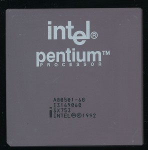
Intel A80501-60 SX753 - Early 1993 containing the FDIV bug

Intel A80501-60 SX753 – Early 1993 containing the FDIV bug

In 1994 Intel had a bit of an issue.  The newly released Pentium processor, replacement for the now 5 year old i486 had a bit of a problem, it couldn’t properly compute floating point division in some cases.  The FDIV instructions on the Pentium used a lookup table (Programmable Logic Array) to speed calculation.  This PLA had 1066 entries, which were mostly correct except 5 out of the 1066 did not get written to the PLA due to a programming error, so any calculation that hit one of those 5 cells, would result in an erroneous result.  A fairly significant error but not at all uncommon, bugs in processors are fairly common.  They are found, documented as errata, and if serious enough, and practical, fixed in the next silicon revision.

What made the FDIV infamous was, in the terms of the 21st century, it went viral.  The media, who really had little understanding of such things, caught wind and reported it as if it was the end of computing.  Intel was forced to enact a lifetime replacement program for effected chips.  Now the FDIV bug is the stuff of computer history, a lesson in bad PR more then bad silicon.

Current Intel processors also suffer from bad math, though in this case its the FSIN (and FCOS) instructions.  these instructions calculate the sine of float point numbers.  The big problem here is Intel’s documentation says the instruction is nearly perfect over a VERY wide range of inputs.  It turns out, according to extensive research by Bruce Dawson, of Google, to be very inaccurate, and not just for a limited set of inputs.

Interestingly the root of the cause is another look-up table, in this case the hard coded value of pi, which Intel, for whatever reason, limited to just 66-bits. a value much too inaccurate for an 80-bit FPU.

October 11th, 2014 ~ by admin

Why the Zilog Z-80’s data pins are scrambled

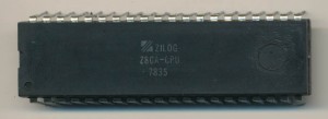
Zilog Z80A CPU -1978

Zilog Z80A CPU -1978

Ken Shirriff has an excellent write up about the Zilog Z80 and why its pin-out, specifically the Data lines, is a bit convoluted.  Rather then being in order (such as D0-D7) the original Z80 is D4,D3.D5,D6,D2,D7,D0,D.  Its functional but its not pretty and can lead to some interesting PCB layout issues.  Ken uses data/imaging from the Visual6502 project to look at the on die reasons for this.  Essentially it came down to saving die space. there literally was not enough room to route the data connections within the confines of the die size.  Keeping the die size small allowed Zilog, and its many second sources), to keep prices down.  In the early days Zilog contracted Mostek to make much of their processors, so die size and the associated cost were a big issue.

Tags:

Posted in:
Research

September 27th, 2014 ~ by admin

Apple A8 Processor: A smaller, faster A7

Anandtech and Chipworks deconstructed an Apple A8 processor, the hear of the new iPhone 6.  By their analysis it is not a radical departure from the A7.  It includes a slightly upgrade, but still quad-core, GPU, and an enhanced dual core ARM processor.  The focus here is clearly on battery performance rather then sheer speed.  Perhaps most interesting is the move from Samsung’s 28nm process to TSMC’s 20nm process (Being made by TSMC will hopefully put to rest the rumors of an Apple/Intel tie up once and for all.).  This results in lower power, a smaller die area, and, assuming yields are on par, a lower cost per chip.  Clock speed appears to be close to the same as the A7 at around 1.3GHz, with most performance improvements being architectural. It would appear to be the smallest improvement in the Apple A series, certainly since the A4->A5.

Considering the incremental improvement from the A7, one can only imagine what Apple has in mind for the A9 which is no doubt well under development.

Tags:

Posted in:
Museum News

September 27th, 2014 ~ by admin

National Semiconductor: The COP before the COPS

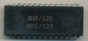
National Semiconductor MM5782N - 400KHz 1976

National Semiconductor MM5782N – 400KHz 1976

In August we detailed the COP2404 and the COP400 line of 4-bit microcomputers by National Semiconductor.  This NMOS design originated in 1977 and was made for over 30 years.  It, however, was not the the first COP line of National Semiconductor.  In fact the COP400 family was referred to as the COPS II for a brief period in the 1970’s.  If the COP400 was the second in line then what was the ORIGINAL COP microcomputer?

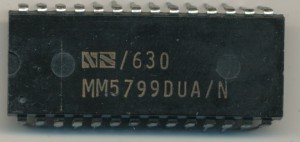
That would be the COPS I of course, better known as the MM5781/2 and its derivatives, the MM5799, MM57140 and MM57152.  These microcomputers were released in 1976 and were made on a volume PMOS process.  They were designed to be inexpensive and simple to use.  The design of the 5781/2 actually started with the MM5734 which was a single chip accumulating calculator chip.  The differences are not as big as one may think.  A multi-function calculator with memory needs an ALU, registers, ann accumulator and instruction decoding, as well as very limited memory and fairly extensive I/O (to run the display and read inputs from the keyboard).  National saw this as an opportunity to capture a bit of the low-end market.  They already had the IMP-16 for their high end, the SC/MP for the mid range, as well as second sourced Intel MCS-4 and MCS-80.  What they lacked was something to compete with the likes of the WD1872 and the TI TMS1000 series as well as the rise of the Japanese 4-bit solutions from NEC, Toshiba and Sanyo.

The 5781/2 was a 2 chip solution, together they formed a microcomputer.  The 5781 contained the program ROM (2048 x 8 bits), as well as the program counter and some control logic.  The 5782 was contained the full ALU, the accumulator, the instruction decoder, and 160×4 bits of RAM.  It could execute 33 different instructions.  Clock speed was 70-400KHz and was provided by an off-chip oscillator.

National Semiconductor MM5799 - Single chip COPs

National Semiconductor MM5799 – Single chip COPs

National combined the 5781/2 into a single 28 pin chip called the MM5799.  It contained all the logic of the 5781/2 but with a smaller amount of RAM (96 x 4 bits) and ROM (1500 x 8 bits). Clock speed remained the same but the instruction set was expanded slightly to 41 instructions.  Two other versions were also made that had more extensive I/O.  The MM57140 which had build in LED drivers, and the MM57152 which was the same, but had built in fluorescent display drivers (this was the 1970’s after all). The ‘140 and ‘152 had 36 instructions 55 x 4 bits of RAM and 630 x 8 bits of ROM. Maximum clock speed was also reduced to 280KHz.

Read More »