September 5th, 2014 ~ by admin

MasPar: Massively Parallel Computers – 32 cores on a chip

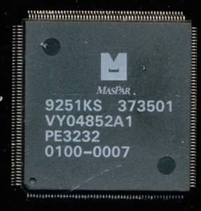
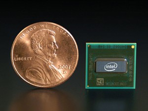
MasPar PE3232 - 32 12.5MHz 32 bit Processing Elements - 1992

MasPar PE3232 – 32 12.5MHz 32 bit Processing Elements – 1992

In the 1980’s DEC researchers were designing a supercomputer based on the Goodyear MPP from 1983.  Jeff Kalb was in charge of the division of DEC involved in this work.  The original Goodyear MPP wa based on a 1-bit processor element (PE).  DEC increased that to a 4-bit PE as well as increased the connectivity between PE’s.  When DEC decided to not commercialize the supercomputer design Kalb left (with DEC’s blessing) to start a company of his own that would.  Thus the creation of MasPar in 1987.

MasPar derives its name from the product it sought to create, a Massively Parallel supercomputer.  These type of computers, also referred to as vector processors are SIMD machines, Single Instruction, Multiple Data.  They perform the same operation on a very large set of data.  SIMD instructions are now found on most all desktop processors, where they can greatly speed up processing of multimedia.  In the late 1980’s there was several companies making such MPP computers.  Perhaps the most famous was Cray, but there was also Thinking Machine’s Connection Machine, Intel’s Paragon (i860 based), nCUBE’s hypercube, Meiko Scientific’s CS-1 (Transputer based) and several others.  Such systems cost from upwards of $100,000 each so sales were not vast, typically companies sold a few hundred to a few thousand systems.

MasPar’s first design, the MP-1 was based directly on the research done at DEC.  Each processing element contained a 4-bit ALU, a 1-bit logic unit, a 64/16 (mantissa/exponent) unit for handling floating point.  Each PE also had 48 32-bit registers.  There were designed as a 32-bit RISC processor, which means, that with the 4-bit ALU, any ALU operation would take at least 8 cycles.  This was considered acceptable in a MPP type system.  Each custom VLSI CMOS MP-1 chip contained 32 individual PE’s.  They were made on a 1.6u process and contained 400,000 transistors.  Clock speed was a fairly low 12.5MHz but this allowed the chips to be air cooled with no special cooling systems.   They were packaged in an inexpensive 208 PQFP, nothing special needed due to the low heat dissipation.  A 1024 PE board (32 chips) dissipated only 50 Watts, and an entire 16k processor system dissipated less than 1,000 watts.

Read More »

August 30th, 2014 ~ by admin

Improve Technologies Make-it 486 – 286 Upgrade

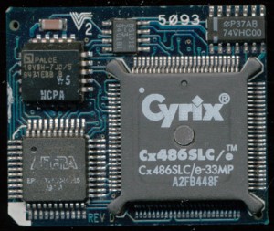
Cx486SLC/e-33MP Based Improve Technologies Make-It 386 for a 286

Cx486SLC/e-33MP Based Improve Technologies Make-It 386 for a 286

Improve Technologies (IT) was a company that existed from 1991-1997.  They were one of the many (to include Cyrix, Evergreen, PNY, Gainbery, etc) that made processors for upgrading 286, 386 and 486 computers.  Processor upgrades are no longer commonplace, becoming nearly non-existent (except for such things as 771 to 775 adapters).  Today computer hardware has become so inexpensive that upgrading more often just consists of purchasing a whole new computer, or at least new motherboard, RAM, and CPU, all at a price of a few hundred dollars.

In the early to mid-90;s however, a computer system cost 2-$3000, so replacing it every few years was not financially viable for many people.  Thus processor upgrades, they were designed to replace a CPU with the next generation CPU (with some limitations) at a price of a few hundred dollars.

In 1976 TranEra was founded in Utah. TransEra is an engineering solutions company, they are built on seeing a technological problem, and engineering a solution, whatever that may be.  They began by making add-on for Tektronix test gear and HP-IB interface equipment.  In 1988 they released HTBasic, a BASIC programming language (based on HP’s Rocky Mountain BASIC) for PC’s.  This is what TransEra became perhaps best known for, as they continue to develop and sell HTBasic.  It was TransEra who developed the Improve Technologies line of upgrades.  They saw a problem, and engineered a solution.

Read More »

Tags:
,

Posted in:
CPU of the Day

August 25th, 2014 ~ by admin

National Semiconductor COP2404 – Dual Core Processor from 1982

National Semiconductor COP2404N - Dual core processor

National Semiconductor COP2404N – Dual core processor

National Semiconductor introduced the COPS series of 4-bit processors in 1977.  COPS came from National’s calculator line of chips, and for a short time were known as Calculator Oriented Processors, however this was rapidly changed to Control Oriented Processor System (COPS).  These 4-bit microcontrollers, as their name suggests, were for controlling various consumer devices.  They were used in all sorts of devices from game consoles, to dishwashers.  In the early 1980s National began producing them in CMOS versions, and in 1988 they extended the line to 8-bit (the COP8 family).

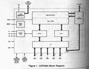
COP2404 Block Diagram - 2 Cores with shared memory. - Click to enlarge

COP2404 Block Diagram – 2 Cores with shared memory. – Click to enlarge

In 1981 the COP2404 (and 2440) were announced, with availability beginning in 1982.  The COP2404 was on the top end of the COPS line, it was found that some real time control operations were better served by 2 microcontrollers, so why not design 2 into one.  The 2404 is a dual core processor, with two complete COPS404 cores on one die, sharing I/O and RAM. (The 2440 also included ROM).  True to multi-core form, the memory was shared, meaning the processors could work independently or pass data to each other, including task handoffs if the programmer so desired.  This wasn’t implemented in hardware, but it wasn’t forbidden either, meaning a programmer could do some pretty complicated task management with the dual CPU cores.

The 2404 was packed in a 48 pin PDIP, and was designed as a development device for use with external program memory (EPROM typically).  Production devices were the 2440 (40 pin) 2441 (28 pin) and 2442 (24 pin) which all had 2K of ROM on die.  All included 160×4 bits of RAM and had an instruction cycle of 4usec (using a 4MHz clock, as each instruction took 16 cycles).  They were manufactured on a 3-micron NMOS process (originally, likely shrunk over time).

As technology progressed it became easier to handle multiple real time tasks with a single, faster controller, with good hardware interrupt handling, but for a time, their was a dual-core processor.  The COPS series continued to be sold by National until 2011, when they were bought by Texas Instruments.  While no longer actively marketed, several members of the COP8 line are still being sold.

August 15th, 2014 ~ by admin

Four-Phase Systems AL1 Processor – 8-bits by Lee Boysel

Four-Phase Systems AL-4 - 1000+ gates 8-bits

Four-Phase Systems AL-4 – 1000+ gates 8-bits

In today’s tech economy there are companies that serve as incubators for startups, such institutions as Y-Combinator and Techstars entire purpose is to help develop emergent tech companies.  In the 1960’s there was also tech incubators, perhaps the best known is Fairchild.  The difference is that Fairchild was not designed to be an incubator, nor were they trying to be.  The bureaucracy of such a large corporation allowed many engineers in somewhat marginal positions to work extensiely on projects of their own. Projects that perhaps were not directly beneficial to Fairchild, but close enough related to slip under managements noses.  Many of the ‘great’ semiconductor companies were started by former Fairchild employees, Robert Noyce, co-founder of Intel, being perhaps the most famous.

Lee Boysel started work at Fairchild in 1966 after working at several other companies semiconductor departments.  Boysel had one main focus, MOS.  MOS (Metal-Oxide-Semiconductors) were very new in the 1960’s and their potential was not well understood.  Most IC’s were designed using Bipolar technology but Boysel saw the potential of MOS and worked at Fairchild to perfect its processes.  He designed a 256-bit RAM in MOS< as well as an 8-bit full adder, as well as the first MOS IC with over 100 gates.  None of these designs were of great commercial success, but that was Fairchild’s problem, not Boysel’s. Boysel was building the foundations for his greater plans, plans that would be realized only after leaving Fairchild.

Boysel left Fairchild in 1968, to build a new company known as Four-Phase Systems.  Four-Phase was named after the 4-phase clocking system used in the MOS logic Boysel had designed.  Boysel’s goal was to build a single chip computer using MOS and use it to power systems to rival the likes of Data General and IBM.  Initial funding of $2 million was provided, somewhat ironically, by Corning Glass works, who also owned a large portion of Signetics.  Initial production of Boysel’s designs was by yet another Fairchild incubated startup known as Cartesian inc.  Cartesian was offered foundry services that duplicated Fairchild;s MOS process.  This saved Four-Phase from having to build there designs for a completely new process.

Read More »

Tags:
,

Posted in:
CPU of the Day

August 13th, 2014 ~ by admin

What’s Missing?

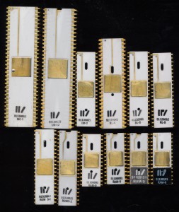
Four-Phase Systems: 1969-1981

Four-Phase Systems: 1969-1981 (click to enlarge

What’s Missing from this Four-Phase Systems family portrait?  Hopefully the lost member arrives this week.  Anyone remember Four-Phase?

Posted in:
Just For Fun

August 10th, 2014 ~ by admin

An Interesting Fujitsu MCM Pentium Module

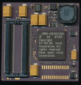
Fujitsu MRN-3545 (100) 100MHz Pentium with no L2 Cache

Fujitsu MRN-3545 (100)
100MHz Pentium with no L2 Cache

We have seen Fujitsu MCM Pentiums before.  120MHz, 133MHz 150MHz and MMX ones.  One is pictured in the article on the MicroModule Systems Gemini here.  The 100MHz module is similar, though it is missing the L2 cache tag RAM (256 kbit chip on the top of the package) as well as the 2 cache RAM chips normally installed on the backside of the module.  It would appear that Fujitsu offered these modules with the cache being optional.  There was a 133MHz version (MRN-3548) with cache, and one (MRN-3549) without cache.

These processors were typically used in environmentally challenging environments.  Panasonic famously used them in their ToughBook CF25, the beginning of a line of highly durable laptop in 1996.  Some of these applications were sealed environments, they did not have vents, or active cooling.  This obviously  makes cooling a challenge.  Removing the L2 cache, while causing a significant hit in performance, would alleviate some of the heat generation.

We consider L2 cache to be essential, but many applications do not require it.  Intel infamously removed the L2 Cache completely from the first Celeron processors and while they worked, they were not particularly competitive performance wise.  When competing against wind, rain dirt, and droppage? L2 cache may not be so important

Posted in:
CPU of the Day

July 10th, 2014 ~ by admin

CPU of the Day: NEC 78C11 Sample and the 78K family

NEC uPD78C11 ES for Mask ROM

NEC uPD78C11 ES for Mask ROM

Most microcontrollers store the program they run in ROM, most of the time this ROM takes the form of a Mask ROM.  This means that its set at the factory when the die is being made, one layer (or more) of the die contains the ROM and the program is hardcoded into the device.  Development versions almost always exist that allow programs to be developed before the mass produced Mask ROM chip, but still the mask must be tested.

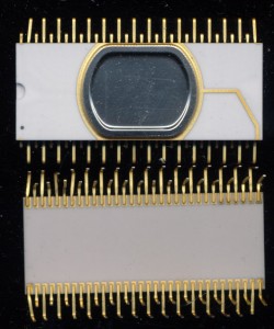
This is such an example from NEC.  It is a engineering sample of a uPD78C11 made in 1988.  the 78C11 (and many others in the 78k family) used a 64 pin QUIP (Quad Inline Package),  The 2 rows of staggered pins allowed for a 64 pin DIP in a much smaller foot print.  The only problem was these chips are extremely delicate.  They were designed to be soldered in and never removed.  The standard package was plastic, but for the sake of testing, these are ceramic (its a bid easier to place/bond the dies on small batches on a ceramic package)

The NEC 78k family was and continues to be very popular.  Its current version (the RL78) is made by Renesas, which was formed when Mitsubishi, Hitachi, and NEC joined their semiconductor businesses.  78K processors powered everything from word processors to washing machines and sewing machines.  Now they are also commonly found in automotive applications.

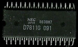
NEC uPD7811G - 1988

NEC uPD7811G – 1988

Like many modern microcontroller families the NEC 78k traces its lineage back to the 1970’s.  The family first appeared in 1980 as the uPD7801.  The 7801 was a microcomputer based on the NEC 780 which was NEC’s version of the Zilog Z80.  The 781x series released in 1982 expanded on the architecture by including an ADC, as well as a full 16-bit ALU (versus the 8-bit from the 780 and 780x) that even supported 16-bit multiply and divide.  The 16-bit ALU made it a simple task for NEC to again extend the architecture to a 16-bit version.  The instruction set was similar, though the naming was different then the Z80.  In 1985 NEC moved the 78k line to a CMOS process, reducing power requirements and increasing the max clock from 12 to 15MHz.

The inclusion of many peripherals made the 78k a popular choice for many embedded applications.  Its continued availability, and wide code base have allowed it to continue to thrive.  And once again, a ‘modern’ MCU is based on a design from the 1970’s.  Processor architectures rarely die, they just continue morphing.

June 12th, 2014 ~ by admin

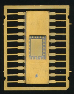
Early Unfinished Ceramic DIP Package

Package 22 CDIP inFrameMost all IC manufacturers do not make their own packaging.  Raw packages are purchased form package suppliers such as Kyocera and NGK (among many others).  The die is installed, bonded, wired, and tested, and then shipped.  This is an early unfinished 22 pin white ceramic DIP.  This is typical construction from the 1960’s and 1970’s.  The package is supplied as a flat, with the leads straight out and unbent.  All the leads are connected by the ‘lead frame’.  The lead frame keeps the leads straight during die placement and handling.  Only once the die is installed, and the bonding wires connected are the leads (soon to be pins) cut free from the lead frame.   The bottom of the die cavity is connected to the ground pin, and the die is affixed to the package with a conductive resin.  Typically one of the pads on the top of the die will also be connected to the same ground pin.

After the die is affixed and wired, the device is tested and the leads are bent to form a standard DIP package.  In some cases the leads are left unbent and the package becomes a type of surface mount package.  A cap is soldered (or s0metimes brazed) over the die cavity, markings applied and then the device is ready to ship.

Tags:

Posted in:
CPU of the Day

May 28th, 2014 ~ by admin

Intel Joins Forces with Rockchip – ARM Meets x86

rockchip logoIt’s well known that Intel missed the jump on tablet and phone processors.  Intel sold off their PXA line of ARM processors to Marvell in 2006, in an attempt to ‘get back to the basics.’  It turned out that this sale perhaps was a bit premature, as the basics ended up being mobile, and mobile is where Intel struggled (by mobile we mean phones/tablets, not laptops, which Intel has no problems with).

In January of 2011 Intel purchased the communications division of Infineon, gaining a line of application and baseband processors, based on ARM architecture of course.  Intel developed this into the SoFIA applications processor, which was ironically fab’d by TSMC.   Eventually the designs would be ported to Intel 14nm process, or that was the plan.

Intel Atom - Now by Rockchip?

Intel Atom – Now by Rockchip?

So this weeks announcement that Intel has signed an agreement with the Chinese company Rockchip, to cooperate on mobile applications processors is a bit of a surprise, but the details show that it makes sense.  Rockchips current offerings are ARM based, much as Intel’s current SoFIA processor, as well as Apple Ax series, Qualcomm’s SnapDragon, TI’s OMAP, etc. However, the agreement with Rockchip is not about ARM, its about x86.  For the first time in many years Intel has granted another company an x86 license, specifically, Intel will help ROckchip build a quad-core Atom based x86 processor with integrated 3G modem.  Rockchip currently uses TSMC as their fab, however also with this agreement Rockchip gets access to Intel 22nm and 14nm fab capacity.

Who wins?

Read More »

May 26th, 2014 ~ by admin

Memorial Day Chip: Motorola 6800/BQCJC 8-Bits of Military spec

Motorola 6800/BQCJC - Mil-spec 6800 from 1985

Motorola 6800/BQCJC – Mil-spec 6800 from 1985

The Motorola MC6800 was Motorola’s first full 8-bit processor.  Introduced in 1974 it was a very good processor, and at the time it did not have a lot of competition, mainly the Intel 8080 and 8008.  Within 2 years though it was competing against the 6502. the 1802, the Z80 and a host of other processors.

This particular example was made in 1985 and is a MIL-STD-883 rated device for use in high reliability military applications.

But the 1980s 8-bit designs were surpassed by 16 and 32-bit designs for most computer use, leaving the 8-bit MC6800 to largely be relegated to use in embedded application and microcontroller work.   Motorola made several version of the 6800 specifically for use as MCUs, the 6802, the widely used 6805 (and its CMOS version the 68HC05) and the 68HC08.  All of which are still in use today, 40 years after Motorola made the first 6800.  The 6800 (and its derivatives also continue to be used as IP cores, read for dropping into ASIC/FPGA designs.  Just this year Digital Core Designs added the 68HC08 to their library of available IP cores.

Tags:

Posted in:
CPU of the Day