April 7th, 2014 ~ by admin
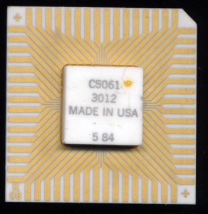
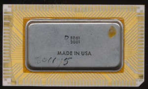
HP C5061-3012 – 16 Bit – 4 MHz – 1984
In last months article on HP’s 16 bit processors we mentioned it was made in a reduced version (on an enhanced NMOS III process). This CPU was known as the C5061-3012. It contains only a BPC (Binary Processor Chip) and no EMC or IOC. It was meant for simpler designs, such as a tape controller, but also in some other HP test equipment. While a simpler implementation, it would seem that HP chose to continue the use of rather beautiful, and highly delicate packaging. This example was made in 1984, a time when most other ICs were grey ceramic or plastic, not a white/gold ceramic package.
This was meant to mounted to a heatsink, which dissipated the heat as well as protected the wafer this ceramic (the package, other than where the die is, is less than 1mm thick)
March 28th, 2014 ~ by admin
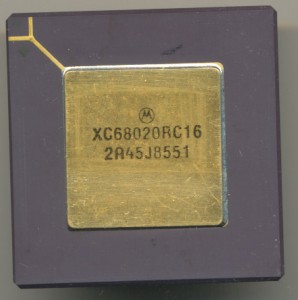
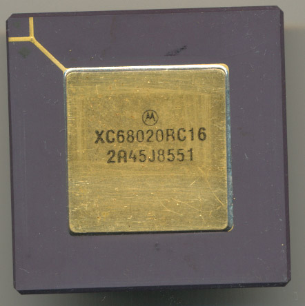
1985 production 68020 ‘XC’ denotes a not fully qualified device.
In 1979 Motorola wow’d the world with the introduction of the MC68000 MACSS (Motorola Advanced Computer System on Silicon). One of the first single chip 32-bit processors. In 1982 the design was upgraded and revised, and released as the 68010. Performance wasn’t that much better then the original 68k so it saw much smaller adoption.
In 1984 Motorola continued the 68k line with the 68020. Speed was greatly improved, up to 33MHz. It was originally made on a 2 micron HCMOS process, allowing the design to use 200,000 transistors and integrate additional addressing modes, co-processor support, and multi-processor support.
The Swedish Computer archeology blog Ehliar has a nice article and die shots on its architecture and design. Check it out.
March 18th, 2014 ~ by admin
HP D5061-3001 – 10MHz 24,000 Transistors
40+ Years after computer processors began to be made, there are several that stick in peoples minds as ‘the greats’ as being somehow more important then others. Processors such as the Intel 4004, the MOS 6502 of Apple fame, and the Motorola 6800 have taken histories podium as the most important.
The truth, however, is a bit different, yet no less exciting. There are those processors that at their time, were vastly ahead of their time, such technological marvels that they continued to be competitive for a decade, impressive today, nearly unheard of in the 1970’s. Some of these processors never saw wide use in PCs, such as the 1802 or SMS300 yet were remarkable. Still others were designed not to be mass market, or to be licensed but to satisfy a company’s internal needs for a processor to power their equipment. These in house designs were every bit as impressive as the competition but since they were used by their creators alone, they faded into obscurity. One such example was the Bell Labs BELLMAC-8, designed by, and for Western Electric. They were not alone however…
Read More »
March 11th, 2014 ~ by admin
IBM z800 MCM
Mainframes are the workhorses of the computing industry. They process transactions for about every industry, and handle the brunt of the economy. Their MTBF (Mean Time Between Failures) is measured in decades (typically 20-50 years). A comparison to a home computer is hard to make, they are in an entirely different league, playing an entirely different game.
Data Intense vs. CPU Intense
Mainframe processors such as these work in what is referred to as ‘Data Intensive’ computing environments. This is different from multi-cored processing that focuses on ‘CPU Intensive’ computing. CPU intense has a relatively small data set, but most perform a lot of work on that set of data, or do the same instruction on a set of data (such as graphics). CPU Intense processing can often be sped up with the addition of more processing cores. Data Intense processing does not see as much benefit from adding cores. Its biggest bottleneck is accessing the data, thus the System z tends to have VERY large caches, and very high bandwidth memory. They typically operate on transactional type data, where the processing has to operate in a certain order (A has to be done before B which has to finish before C etc).
IBM was one of the first, and continues to be one of the largest suppliers of such systems. Starting with the System/360 introduced in 1964 to the zSeries today. The zSeries was first launched in 2000 with the z900, a significant upgrade from the System/390. Data addressing was moved to 64-bits (from 31 bits) yet backwards compatibility (all the way back to the 360) is maintained. The z900 ran at 775MHz and was built with a 35 die MCM containing 20 Processing Units (PUs) and 32MB of L2 Cache.
Read More »
March 6th, 2014 ~ by admin

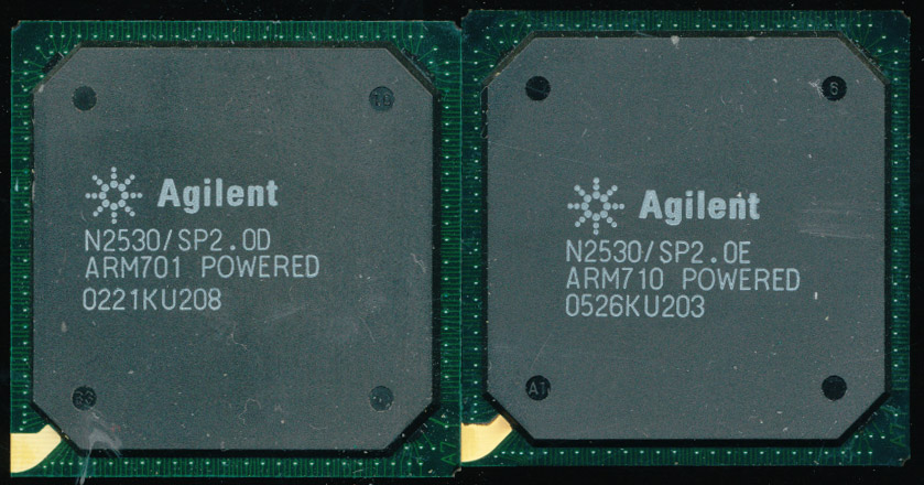
ARM 701 mis-print on the left
We recently received several Remote Server management cards, powered by the Agilent (spun off of HP in 1999) N2530 SoC. This SoC provides the processing for remotely administering, and managing servers. At its hearts is an ARM processor running at 33MHz. Proudly marked on the chip, is ‘ARM 701 POWERED.’ There is one problem, there never was an ARM701 processor core. The N2530 is in fact powered by an ARM710. A typo was made when marked the Rev D chips, and later fixed on the Revision E. I have not yet received an example of a Rev C (or earlier) to see if they too have this error, but E and later certainly did not. The Agilent N2530 was used for many years in the early 2000’s on cards by Dell, Fujitsu, and IBM (and likely others). Essentially forming a computer within a computer, these cards often had their own graphics support (ATI Mobility Radeon, among others) as well as support for CD-ROMs, hard drives, LAN (for access) and everything else you would find in a stand alone computer. Typically they could remote start, reboot, and power down servers, all over a network connection.
February 27th, 2014 ~ by admin
Bloomberg Business Week recently published an interesting article on ARM’s rise to power in the processing world. There first major design ‘win’ was a failed product known as the Apple Newton, yet they would go on to become a powerhouse that is no challenging Intel.
In ARM’s formative years, the 1990’s, the most popular RISC processor was the MIPS architecture, which powered high end computers by SGI, while Intel made super computers (the Paragon) based on another RISC design, the i860. Now, nearly 2 decades later, after Intel abandoned their foray into the ARM architecture (StrongARM and X-Scale) RISC is again challenging Intel in the server market, this time, led by ARM.
MIPS, now owned by Imagination, is again turning out new IP cores to compete with ARM, and other embedded cores. Their Warrior class processors are already providing 64-bit embedded processing power, though with a lot less press that the likes of Apple’s A7.
February 18th, 2014 ~ by admin
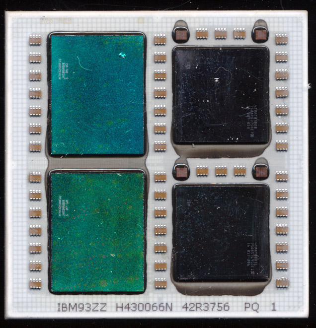
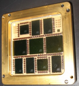
IBM POWER5+ QCM – 4 dies, 8 cores, and 72MB of L3 Cache
When the POWER5 processor was released in 2004 it was made in two versions, a DCM (Dual Chip Module) containing a POWER5 die and its 36MB L3 cache die, as well as a MCM containing 4 POWER5 die and 4 L3 cache dies totaling 144MB. The POWER5 is a dual core processor, thus the DCM was a dual core, and the MCM an 8 core processor. The POWER5 contains 276 million transistors and was made on a 130nm CMOS9S process.
In 2005 IBM shrank the POWER5 onto a 90nm CMOS10S manufacturing process resulting in the POWER5+. This allowed speeds to increase to 2.3GHz from the previous max of 1.9GHz. The main benefit from the process shrink was less power draw, and thus less heat. This allowed IBM to make the POWER5+ in a QCM (Quad Chip Module) as well as the previous form factors. The QCM ran at up to 1.8GHz and contained a pair of POWER5+ dies and 72MB of L3 Cache.
The POWER5+ was more then a die shrink, IBM reworked much of the POWER5 to improve performance, adding new floating point instructions, doubling the TLB size, improved SMP support, and an enhanced memory controller to mention just a few.
The result? A much improved processor and a very fine looking QCM.
February 9th, 2014 ~ by admin
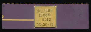
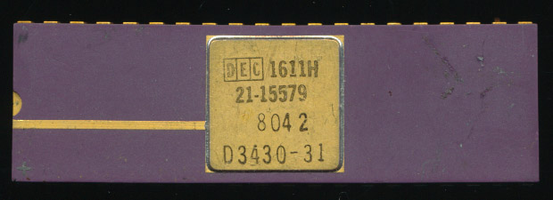
DEC 1611H 21-15579 – LSI-11 RALU (MCP-1600)
Fully 10 years before Western Digital released their first hard drive, they made processors, calculator chips, Floppy Disk controllers and a host of other IC’s. Western Digital began in 1970 making primarily calculator chips. In 1976 they announced the multi-chip MCP-1600 processor. This was an implementation of the PDP-11 minicomputer in silicon. It consisted of a CP1611 Register/ALU chip, a CP1621 control chip and either 2 or 4 CP1631 512x 22bit MICROMs that contained the microcode implementation of the PDP-11 architecture. Physically this was an 8-bit design, but clever microcode programming allowed it to function as a 16-bit processor. Use of microcode allowed it to also implement floating point support, a very new concept in hardware in 1976. The MCP-1600 was used in DECs LSI-11 microcomputer among others.
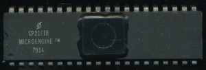
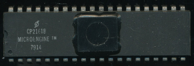
Western Digital CP2161B – 1979 Pascal Control Chip
Having the microcode separate from the ALU/Control didn’t help with board layout or cost, but it did provide a very flexible platform to implement other architectures on. In the late 1970s UCSD (University of California in San Diego) was working on a project, led by Kenneth Bowles, to make a portable version of the Pascal programming language, a version that could run on multiple hardware platforms, very similar to how Java has become today. The code was compiled to a ‘p-code’ or pseudo code that could them be executed by a virtual machine onto whatever hardware. Typically this virtual machine would be implemented in software, however the design of the MCP-1600 was such that it could be implemented in hardware, or rather microcode. Thus in 1978, the WDC MICROENGINE was born. This was to be a 5 chip set (original documentation states 4, but it ended up being 5) that consisted of the CP2151 Data chip (if you have a CP2151 you would like to donate, let us know) , the CP2161 Control chip, and 3 512 x 22 bit MICROMs which contained the microcode to directly execute UCSD Pascal on the data chip. The CP2151 was no different from the CP1611 of the MCP-1600 chipset and could be interchanged.
Read More »
January 20th, 2014 ~ by admin
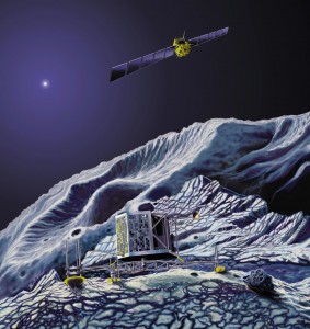
Rosetta Comet Chaser – Dynex 1750
The ESA’s comet chaser Rosetta has just today awoken from a long deep sleep on its comet chasing (and landing) mission. The solar powered spacecraft was launched back in 2004. It is based on the Mars Mariner II (itself based on the Voyager and Galileo) spacecraft design of the early 1990s (when the mission was first conceived.) Main differences include using very large solar arrays versus a RT (Radioisotope Thermal Generator) and upgraded electronics.
In order to conserve power on its outward loop (near Jupiter’s orbit) most all systems were put to sleep in June of 2011 and a task set on the main computer to waken the spacecraft 2.5 years later and call home. The computer in charge of that is powered by a Dynex MAS31750 16-bit processor running at 25MHz, based on the MIL-STD-1750A architecture.
A reader recently asked why such an old CPU design is still being used rather then say an x86 processor. As mentioned above the Rosetta design was began in the 1990’s, the 1750A was THE standard high reliability processor at the time, so it wasn’t as out of date as it is now that its been flying through space for 10 years (and 10 years in the clean room). The 1750A is also an open architecture, no licenses are or were required to develop a processor to support it (unlike x86). Modern designs do use more modern processors such as PowerPC based CPUs like the RAD750 and its older cousin the RAD6000. Space system electronics will always lag current tech due to the very long lead times in their design (it may be 10 years of design n the ground before it flies, and the main computer is selected early on). x86 is used in systems with 1) lots of power, and 2) somewhat easily accessible. Notably the International Space Station and Hubble. x86 was not designed with high reliability and radiation tolerance in mind, meaning other methods (hardware/software) have to be used to ensure it works in space.
Currently the ESA designs with an open-source processor known as the LEON, which is SPARC-V8 based.
January 17th, 2014 ~ by admin
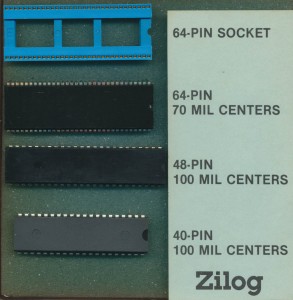
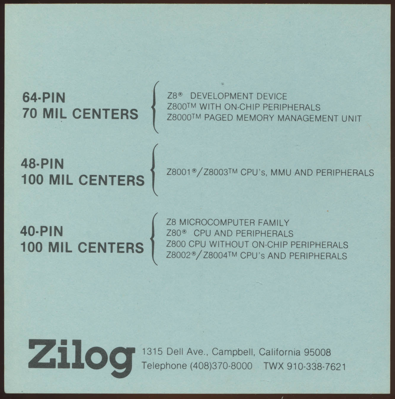
Zilog Packages available in 1985
Last week we showed you an educational kit from Zilog showing the process involved in making and assembling a Z80 processor, from polished wafer to packaging. Zilog also made a kit for marketing the various packages used. This kit contains a shrink DIP 64 pin socket, a shrink DIP 64pin package, a 48 pin DIP and 40 pin DIP, all the common packages used at the time.
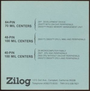
Zilog Packages – Z8 Z80 Z800 and Z8000
At the time is a little hard to track down as no date is provided with this kit. We can get very close though looking at the back where Zilog lists which devices are available in these packages. The usual Z80 and Z8000 series are both there as well as the Z8 microcontroller family. The one odd-ball is the Zilog Z800. The Z800 was an upgraded Z80 released in 1985, adding on chip cache an MMU and a vastly expanded instruction set (over 2000 instruction/addressing modes). It was wholly unsuccessful partly do to bad marketing by Zilog, and partly because it did more then it needed to. It never entered mass production, and by 1986 Zilog has redesigned it, converted the design to CMOS (from NMOS) and released it as the Z280 which met the same fate as the Z800. It seemed that making an overly complicated Z80 wasn’t what the market wanted. THe Z180 (designed by Hitachi) and the Zilog eZ80 (released in 2001), have enjoyed much wider success, mainly because they kept closer to the simplicity of the original Z80.
So when was this kit put together? Likely 1985, as the Z800 was nly talked about for a few months before quietly being put away.