February 9th, 2014 ~ by admin

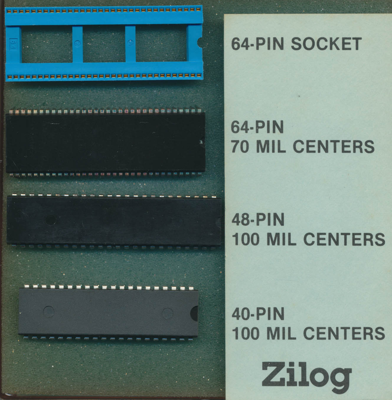
Western Digital WD/9000 Pascal MicroEngine

DEC 1611H 21-15579 - LSI-11 RALU (MCP-1600)

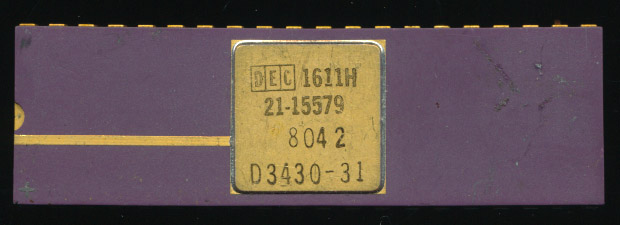
DEC 1611H 21-15579 – LSI-11 RALU (MCP-1600)

Fully 10 years before Western Digital released their first hard drive, they made processors, calculator chips, Floppy Disk controllers and a host of other IC’s.  Western Digital began in 1970 making primarily calculator chips.  In 1976 they announced the multi-chip MCP-1600 processor.  This was an implementation of the PDP-11 minicomputer in silicon.  It consisted of a CP1611 Register/ALU chip, a CP1621 control chip and either 2 or 4 CP1631 512x 22bit MICROMs that contained the microcode implementation of the PDP-11 architecture.   Physically this was an 8-bit design, but clever microcode programming allowed it to function as a 16-bit processor.  Use of microcode allowed it to also implement floating point support, a very new concept in hardware in 1976.  The MCP-1600 was used in DECs LSI-11 microcomputer among others.

Western Digital CP2161B - 1979 Pascal Control Chip

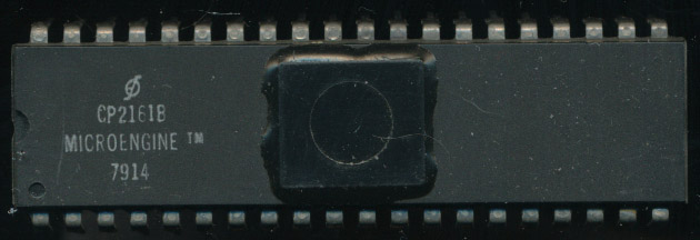
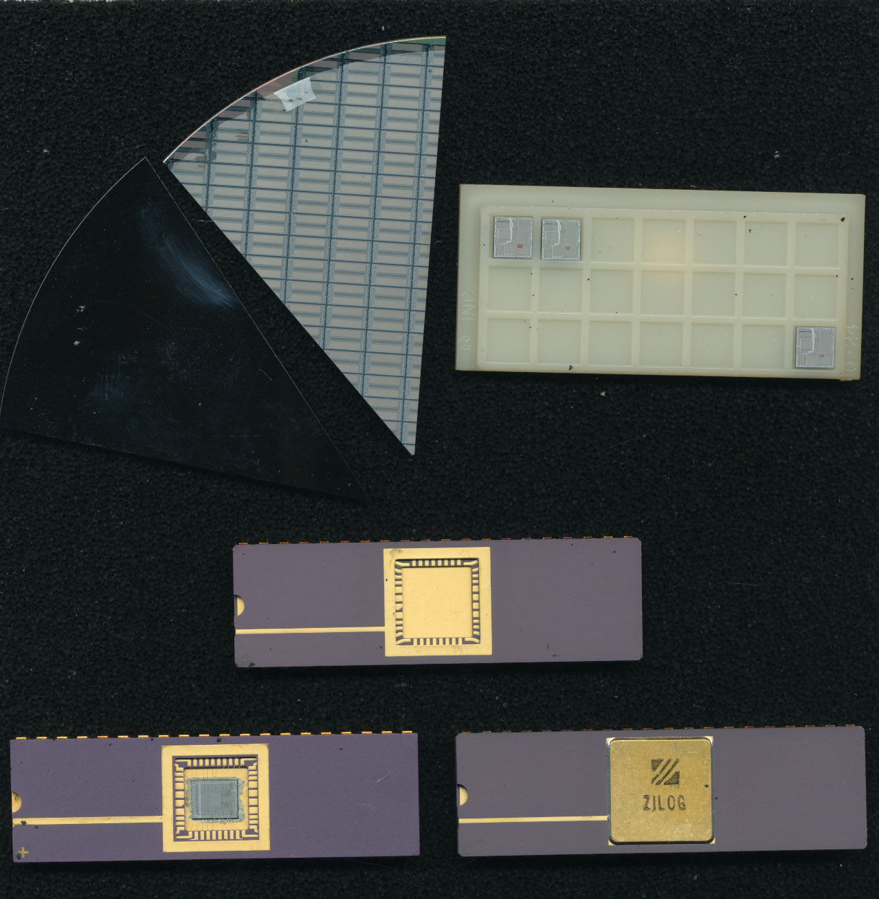
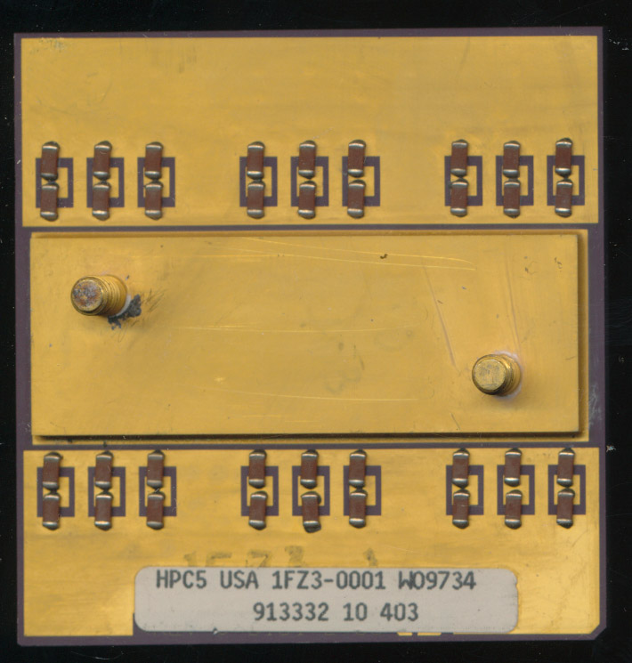
Western Digital CP2161B – 1979 Pascal Control Chip

Having the microcode separate from the ALU/Control didn’t help with board layout or cost, but it did provide a very flexible platform to implement other architectures on.  In the late 1970s UCSD (University of California in San Diego) was working on a project, led by Kenneth Bowles, to make a portable version of the Pascal programming language, a version that could run on multiple hardware platforms, very similar to how Java has become today.  The code was compiled to a ‘p-code’ or pseudo code that could them be executed by a virtual machine onto whatever hardware.  Typically this virtual machine would be implemented in software, however the design of the MCP-1600 was such that it could be implemented in hardware, or rather microcode.  Thus in 1978, the WDC MICROENGINE was born.  This was to be a 5 chip set (original documentation states 4, but it ended up being 5) that consisted of the CP2151 Data chip (if you have a CP2151 you would like to donate, let us know) , the CP2161 Control chip, and 3 512 x 22 bit MICROMs which contained the microcode to directly execute UCSD Pascal on the data chip.  The CP2151 was no different from the CP1611 of the MCP-1600 chipset and could be interchanged.

Read More »

Posted in:
CPU of the Day

January 20th, 2014 ~ by admin

Welcome Back Rosetta: The Dynex MAS31750 Awakens

Rosetta Comet Chaser - Dynex 1750

Rosetta Comet Chaser – Dynex 1750

The ESA’s comet chaser Rosetta has just today awoken from a long deep sleep on its comet chasing (and landing) mission.  The solar powered spacecraft was launched back in 2004.  It is based on the Mars Mariner II (itself based on the Voyager and Galileo) spacecraft design of the early 1990s (when the mission was first conceived.)  Main differences include using very large solar arrays versus a RT (Radioisotope Thermal Generator) and upgraded electronics.

In order to conserve power on its outward loop (near Jupiter’s orbit) most all systems were put to sleep in June of 2011 and a task set on the main computer to waken the spacecraft 2.5 years later and call home.  The computer in charge of that is powered by a Dynex MAS31750 16-bit processor running at 25MHz, based on the MIL-STD-1750A architecture.

A reader recently asked why such an old CPU design is still being used rather then say an x86 processor.  As mentioned above the Rosetta design was began in the 1990’s, the 1750A was THE standard high reliability processor at the time, so it wasn’t as out of date as it is now that its been flying through space for 10 years (and 10 years in the clean room).  The 1750A is also an open architecture, no licenses are or were required to develop a processor to support it (unlike x86). Modern designs do use more modern processors such as PowerPC based CPUs like the RAD750 and its older cousin the RAD6000.  Space system electronics will always lag current tech due to the very long lead times in their design (it may be 10 years of design n the ground before it flies, and the main computer is selected early on).  x86 is used in systems with 1) lots of power, and 2) somewhat easily accessible.  Notably the International Space Station and Hubble.  x86 was not designed with high reliability and radiation tolerance in mind, meaning other methods (hardware/software) have to be used to ensure it works in space.

Currently the ESA designs with an open-source processor known as the LEON, which is SPARC-V8 based.

January 17th, 2014 ~ by admin

Zilog Packaging Marketing Kit

Zilog Packages available in 1985

Zilog Packages available in 1985

Last week we showed you an educational kit from Zilog showing the process involved in making and assembling a Z80 processor, from polished wafer to packaging.  Zilog also made a kit for marketing the various packages used.  This kit contains a shrink DIP 64 pin socket, a shrink DIP 64pin package, a 48 pin DIP and 40 pin DIP, all the common packages used at the time.

Zilog Packages - Z8 Z80 Z800 and Z8000

Zilog Packages – Z8 Z80 Z800 and Z8000

At the time is a little hard to track down as no date is provided with this kit.  We can get very close though looking at the back where Zilog lists which devices are available in these packages.  The usual Z80 and Z8000 series are both there as well as the Z8 microcontroller family.  The one odd-ball is the Zilog Z800.  The Z800 was an upgraded Z80 released in 1985, adding on chip cache an MMU and a vastly expanded instruction set (over 2000 instruction/addressing modes).  It was wholly unsuccessful partly do to bad marketing by Zilog, and partly because it did more then it needed to. It never entered mass production, and by 1986 Zilog has redesigned it, converted the design to CMOS (from NMOS) and released it as the Z280 which met the same fate as the Z800.  It seemed that making an overly complicated Z80 wasn’t what the market wanted.  THe Z180 (designed by Hitachi) and the Zilog eZ80 (released in 2001), have enjoyed much wider success, mainly because they kept closer to the simplicity of the original Z80.

So when was this kit put together? Likely 1985, as the Z800 was nly talked about for a few months before quietly being put away.

Posted in:
CPU of the Day

January 9th, 2014 ~ by admin

Zilog Educational Sample Kit

Zilog Z-80 Kit - Click for full size

Zilog Z-80 Kit – Click for full size

Here is a neat kit from Zilog.  Its an Educational Kit showing some of the steps of producing a Z-80 processor.  It includes:

  • A raw polished wafer slice before any etching has occured.  This is what a processor starts out with (sliced from a single large ingot)
  • A slice of an etched wafer.  In this case it appears to be some sort of memory, but the process is the same for a processor.
  • Several cut die, these are cut from a wafer after testing.  The red dot notes that these particular dice failed one or more of the tested and should be discard.  Thats probably why they made it into this kit rather then a saleable device.
  • An bare unfinished package.  These packages are rarely if ever made by the company making the processor.  They are made by companies such as NGK (who also makes spark plugs) and Kyocera.  The bottom of the die cavity is usually connected to the ground pin of the package.
  • Next is a package with the die placed in the die cavity.  No bonding wires are installed in this example but that would be the next step.  The very fine gold bonding wires connect the pad ring on the edge of the die, to the pads in the die cavity.  Those [ads are connected through the package to the 40 pins of the ceramic DIP package.
  • Finally we have a completed device.  The lid is usually soldered or brazed onto the package and markings applied.  The marking on this example make it a ‘Marketing Sample’ as they are there solely for looks, rather then to identify the device, its date, and lot.

These types of kits were produced for educational use, and given to schools, as well as sales people to assist in marketing Zilog’s various products

Tags:
,

Posted in:
CPU of the Day

January 6th, 2014 ~ by admin

HP PA-RISC PA-7000 – Multichip RISC

HP 1FZ3-0001 PA7000 66MHz - 1991

HP 1FZ3-0001 PA7000 66MHz – 1991

Welcome to 2014 and a new year of exciting processors and technology finds at the CPU Shack Museum.  We’ll spend the next couple weeks posting some of the more interesting finds of 2013 that didn’t get posted before.

The PA-RISC was HP’s architecture meant to unify all their non x86 processors of the 1980’s.  The project began in the 1980’s and produced over a dozen processors designs, ending with the PA-8900 in 2005, though the Itanium borrows heavily from the PA-RISC line.  HP discontinued support for PA-RISC servers in 2013 and recently announced that they will discontinue use of the Itanium as well.

Early PA-RISC processors were multi-chip designs such as this PA-7000. The PA-7000 pictured is only the CPU, the FPU was a separate chips, as was the L1 caches (no support for L2 caches). A memory controller was also a separate chip.  Made on a 1 micron process the PA-7000 had 580,000 transistors and ran at 66MHz.  Early versions had 2 lugs for the heatsink on the package while later versions had only a single lug.

Posted in:
CPU of the Day

November 19th, 2013 ~ by admin

MAVEN To Mars: Another BAE RAD750 CPU

MAVEN to Mars - RAD750 Powered

MAVEN to Mars – RAD750 Powered

NASA has successfully launched the $671 million MAVEN mission to Mars for atmospheric research.  Like the Mars Reconnaissance Orbiter it is based on, it’s main computer is a BAE RAD750,  a radiation hardened PowerPC 750 architecture.  This processor first flew on the Deep Impact Comet chaser and is capable of withstanding up to 1 million rads of radiation.  The entire processor sub-system can handle 200,000 rads.  To put this in perspective, 1000 rads is considered a lethal dose for a typical human.  Likely much higher then a Apple Mac G3 that the PowerPC 750 was originally used in back in 1998 as well.   The processor can be clocked at up to 200MHz though often will run slower for power conservation.

The MAVEN should reach Mars within a few days of the Indian Space Agency’s $71 million Mangalyaan Orbiter launched earlier this month.  MAVEN is taking a faster route, at the expense of a heavier booster and larger fuel consumption.  The Mangalyaan Orbiter’s main processor is the GEC/Plessey (Originally produced by Marconi and now Dynex) MAR31750, a MIL-STD-1750A processor system.

November 17th, 2013 ~ by admin

Itanium is Dead – And other Processor News

Itanium Sales Forecasts vs Reality

Itanium Sales Forecasts vs Reality

‘Itanium is dead’ is a phrase that has been used for over a decade, in fact many claimed that the Itanium experiment was dead before it even launched in 2001.  The last hold-out of the Itanium architecture was HP, likely because the Itanium had a lot in common with its own PA-RISC.  However HP has announced that they will be transitioning their NonStop sever series to x86, presumably the new 15-core Xeons Intel is developing.  Itanium was launched with goal of storming the server market, billed as the next greatest thing, it failed to make the inroads expected, largely due to the 2 decades of x86 code it didnt support, and poor initial compiler support.  Many things were learned from Itanium so though it will become but a footnote, its technology will live on.

Interestingly other architectures that seemed to be n the brink are getting continued support in new chips.  Imagination, known for their graphics IP, purchased MIPS, and now has announced the MIPS Warrior P-class core.  This core supports speeds of over 2GHz, and is the first MIPS core with 128 bit SIMD support.

Broadcom, historically a MIPS powerhouse, has announced a 64-bit ARM server class processor with speeds of up to 3GHz. Perhaps ironic that ARM is now being introduced into a market that Itanium was designed for. Broadcom has an ARM Architecture license, meaning they can roll their own designs that implement the ARM instruction set, similar to Qualcomm and several others.

POWER continues to show its remarkable flexibility.  Used by IBM in larger mainframes in the POWER7 and POWER8 implementations it crunches data at speeds up to 4.4GHz.  On the other end of the spectrum, Freescale (formerly Motorola, one of the developers of the POWER architecture) has announced the 1.8GHz quad-core QorIQ T2080 for control applications such as networking, and other embedded use.  These days the POWER architecture is not often talked about, at least in the embedded market, but it continues to soldier on and be widely used.  LSI has used it in their Fusion-MPT RAID controllers, Xilinx continues to offer it embedded in FPGAs and BAE continues to offer it in the form of the RAD750 for space-based applications.

Perhaps it is this flexibility of use that has continued to allow architectures to be used.  Itanium was very focused, and did its one job very well. Same goes for the Alpha architecture, and the Intel i860, all of which are now discontinued.  ARM, MIPS, POWER, x86 and a host of MCU architectures continue to be used because of their flexibility and large code bases.

So what architecture will be next to fall? And will a truly new architecture be introduced that has the power and flexibility to stick around?

Tags:
, , ,

Posted in:
Processor News

November 1st, 2013 ~ by admin

nCube and the Rise of the HyperCubes

nCube/2 Processor - 20MHz The logo is a tesseract - 4-way Hypercube

nCube/2 Processor – 20MHz
The logo is a Tesseract – a 4-way Hypercube

In 1983 Stephen Colley, Dave Jurasek, John Palmer and 3 others from Intel’s Systems Group left Intel, frustrated by Intel’s seeming reluctance to enter the then emerging parallel computing market.  They founded a company in Beaverton, Oregon known as nCube with the goal of producing MIMD (Multiple Instruction Multiple Data) parallel computers.  In 1985 they released their first computer, known as the nCube/10.  The nCube/10 was built using a custom 32-bit CMOS processor containing 160,000 transistors and running initially at 8MHz (later increased to 10).  IEEE754 64-bit floating point support  (including hardware sqrt) was included on chip.  Each processor was on a module with its own 128KB of ECC DRAM memory (implemented as 6 64k x 4 bit DRAMs.)  A full system, with 1024 processor nodes, had 128MB of usable memory (160MB of  DRAM counting those used for ECC).  From the outset the nCube systems were designed for reliability, with MTBFs of full systems running in the 6 month range, extremely good at the time.

The nCube/10 system was organized in a Hypercube geometry, with the 10 signifying its ability to scale to a 10-way Hypercube, also known as a dekeract.  This architecture allows for any processor to be a maximum of 10-hops from any other processor.  The benefits are greatly reduced latency in cross processor communication.  The downside is that expansion is restricted to powers of 2 (64, 128, 256, 512 etc) making upgrade costs a bit expensive as the size scaled up.  Each processor contained 22 DMA channels, with a pair being reserved for I/O to the host processor and the remaining 20 (10 in + 10 out) used for interprocessor communication.  This focus on a general purpose CPU with built in networking support is very similar to the Inmos Transputer, which at the time, was making similar inroads in the European market.  System management was run by similar nCube processors on Graphics, Disk, and I/O cards.  Programming was via Fortran 77 and later C/C++. At the time it was one of the fastest computers on the planet, even challenging the almighty Cray.  And it was about to get faster.

Read More »

October 25th, 2013 ~ by admin

Honeywell 1750A-5V: MIL-STD-1750A Lives On

Honeywell 1750A-5V -2008

Honeywell 1750A-5V -2008

While its not in the best condition I was still pleased when it came in.  MIL-STD-1750A was first developed in 1980 to provide a uniform architecture for military computing, while allowing competition in the market to produce different versions at a hoped for reduced cost.  By 1996 though the 1750A was declared inactive for new designs in the US military.  It had been widely replaced by other more powerful commercial designs, notably the 80386 and 80486.  Many militaries around the world continue to use the 1750A and the US Military continues to need spares.

Honeywell continues to produce the 1750A-5V, a single chip implementation of the 1750A with on-board 40-bit FPU, much like Fairchild’s commercial F9450.  Produced on a CMOS SOI (SIlicon On Insulator) 0.65u process the 1750A-5V runs at up to 40MHz, twice as fast as most did in the 1980’s.  This particular example was produced in 2008 though Honeywell continues to make and advertise the 1750A.

The radiation hardened version was used on the Cassini Orbiter (now orbiting Saturn), ESA’s Rosetta Comet probe as well as the Guidance computer for the Air Force’s Titan 4 missile.

October 8th, 2013 ~ by admin

When a Pentium 166 isn’t a Pentium 166

Pentium 166 Faked from Mobile 120

Pentium 166 SY016 Faked from Mobile 120 SY027

Here is an interesting example of what led Intel (and other manufacturers) to start locking down multipliers on their processors as well as adding anti-counterfeiting measures.  This processor appears to be a 166MHz Pentium Processor, which in 1997 sold for around $200.   A 120MHz Mobile Pentium sold for less than $100.  Thus processors of lower speeds were often remarked by unscrupulous dealers and sold as higher speed parts.   The forgeries had to be made quick, as processor prices dropped very quickly, the 166MHz Pentium debuted at nearly $1000.  Most Pentium fakes were made by painting over the original markings and painting/engraving news ones.  Some of the better fakes ground down the old markings first.  Nearly all are easy to spot by the trained eye, wrong fonts, date mismatches, etc.

This particular example, from somewhere in 1997, was faked from a Pentium 120MHz mobile to a 166MHz desktop Pentium.  As far as fakes go this was a fairly conservative one.  Often 166s were faked from 100s or even 75s.  The 120 was a 2x60MHz processor running at 3.1V, while the 166 is 2.5×66 (you see why locking the multiplier discouraged faking?) running at 3.3V.  This resulted in a 28% overclock at about a 6% voltage increase.  In this case the processor likely ran fairly well, if perhaps a bit warm.  Some of the more extreme fakes resulted in very unstable systems due to overheating and pushing a processor well beyond what it was designed for.

Before removing paint

Before removing paint

Today counterfeit chips are still a major problem, though it was shifted from the consumer market, where prices are generally low, to the military and industrial market, where prices are high, and there is still demand for older devices.