October 6th, 2013 ~ by admin
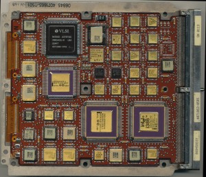
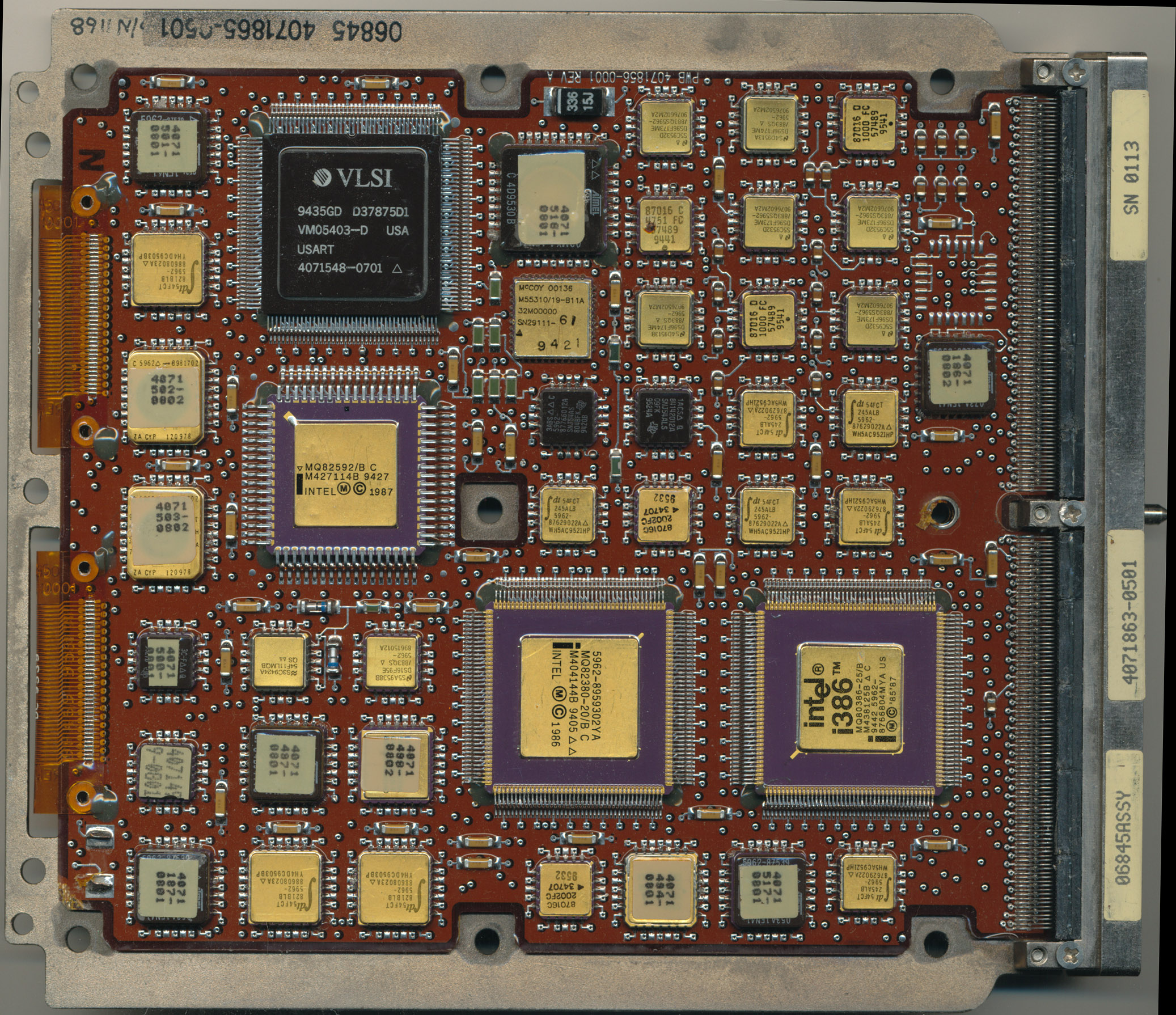
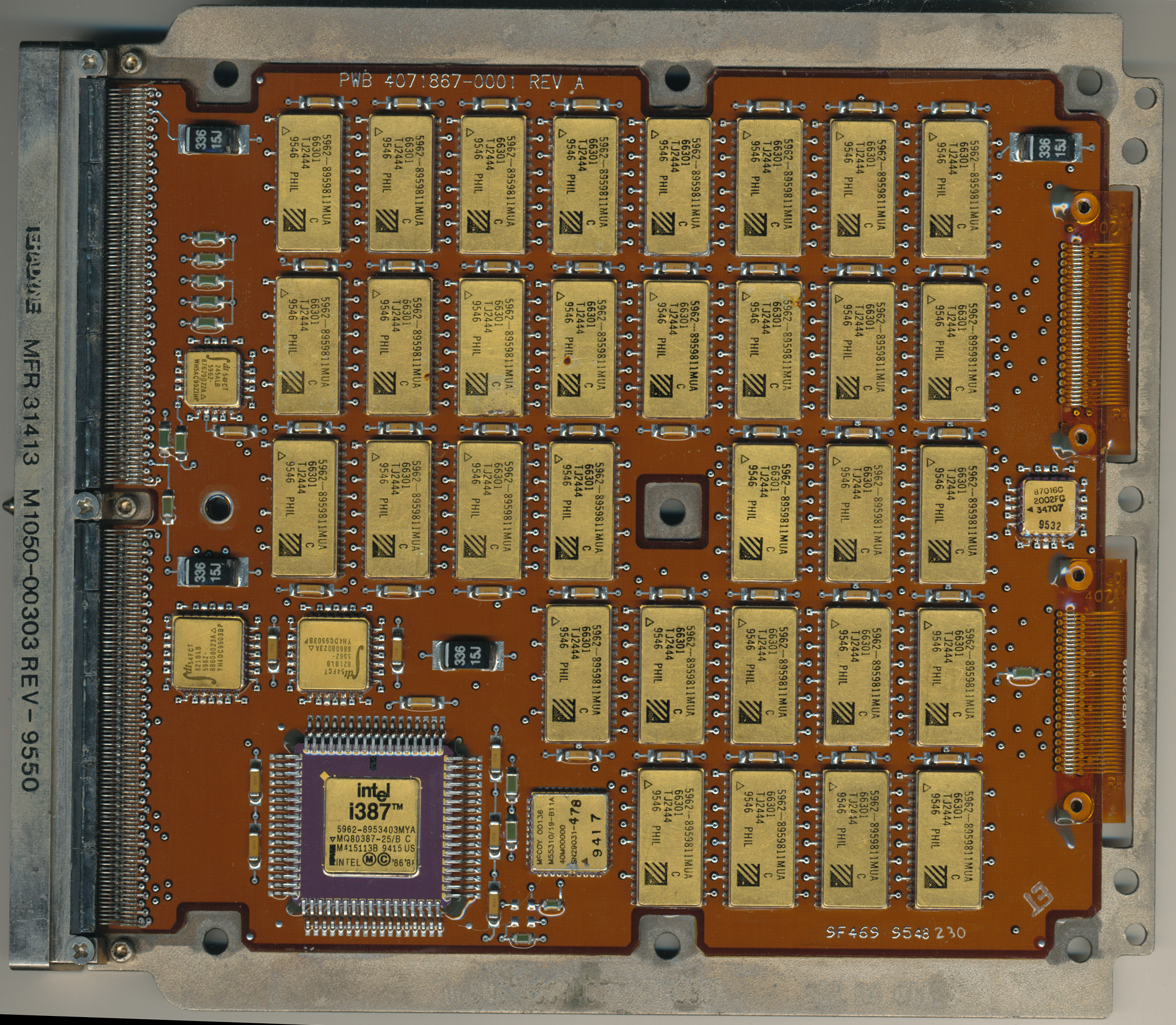
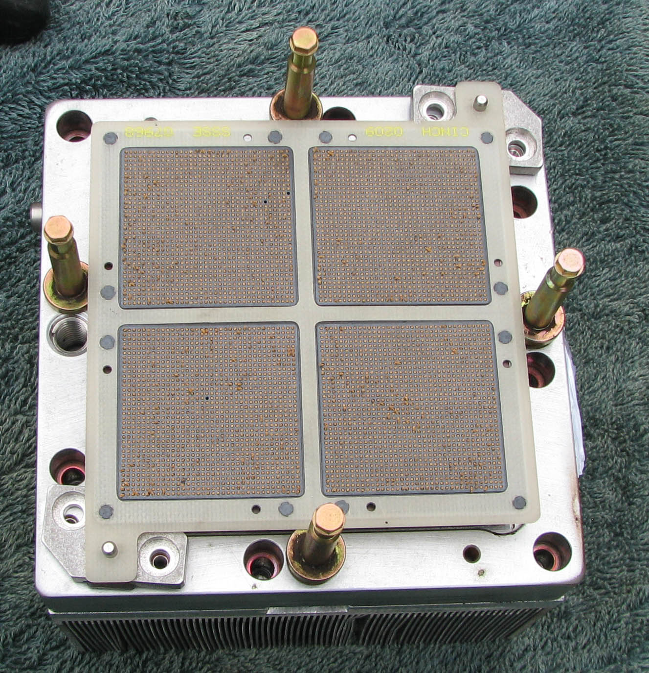
Raytheon KGV-25 – Click to Enlarge
Sometimes we get processors in on boards that are just too interesting, or too good looking to remove. That is the case with this KGV-25 correlator board. It is a processing systems used for decrypting communications that was in wide use by the US (and likely other) militaries in the 1990’s. The KGV-25 could receive encrypted UHF data at rates of up to 400Mbps as part of the Multi-Mission Advanced Tactical Terminal (MATT). More information on the MATT can be found here on the FAS website.
As is typical of military equipment the system did not use the latest and greatest available at the time (this board is from 1994 so the Pentium era). The board is run by a time proven and reliable Intel 80386 processor running at 25MHz. In addition to the MQ80386-25/B (MIL-STD-883B spec 386 processor) the board contains:
Intel MQ82380-20/B – DMA Controller for interfacing with all the assorted SRAM on the board
Intel MQ82592/B – LAN Controller for interfacing with the rest of the system
VLSI VM05403 USART – Universal Asynch/Synch Receiver Transmitter
and on the back is a MQ80387-25/B Math-coprocessor for the 386 and 4MB of 35ns SRAM
Essentially a complete 80386 system, of similar performance to a higher end system int he late 1980’s. Just with a lot more gold, and built to take a lot more abuse then your average beige box of the 80’s
September 28th, 2013 ~ by admin
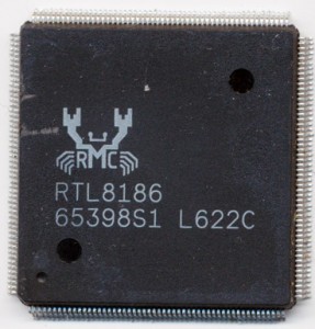
Realtek RTL8186 Lexra LX5280 MIPS with DSP Extensions – 2006
The MIPS architecture was created in 1985 from a project at Stanford University. It was one of the first licenseable architectures. A company could buy a license and make their own MIPS architecture processors. By the 1990’s this had become fairly common and many companies were making MIPS processors, including Performance Semiconductor, IDT, NEC, Toshiba, LSI and more. In 1992 MIPS Computer Systems, Inc. was bought by SGI, in order to guarantee a supply a continued development of new MIPS designs for SGIs computers. It did continue to license the design to other companies as well, fostering competition which helped lower prices for SGI. In 1998 SGI spun off MIPS into its own company once again, as SGI at the time had decided to move towards Intel’s Itanium architecture (this should sound familiar, DEC and the Alpha suffered the same fate). By 2008 MIPS was losing money and in 2013 what little remained (having used most of their cash to buy, and then sell at a loss Chipidea) of them was bought by Imagination Technologies (makers of the PowerVR line of graphic solutions, used notably in the Apple iPhone’s A4, A5, A6, and likely A7 processors). But there is a bit more to the story of MIPS, a seemingly small chapter that very well could have changed history and certainly changed the success of MIPS.
In 1997 a small company called Lexra was started. Lexra was a semiconductor Intellectual Property company. They designed processors and licensed the designs. What made Lexra different is that they designed and licensed soft-cores. A soft core is an RTL (Register Transfer Level) model of the processor. It is usually written and delivered in an HDL (Hardware Descriptive Language) such as Verilog or VHDL and the purchaser may compile it down to whatever actual transistor level hardware they like. This is exactly how ARM works today, but in 1997 ARM only licensed hard cores, cores already compiled down to the gate level and ready for implementation on a given fab process technology. This allowed them to have tighter control over the design and its performance, but made integration much harder into other products. A soft core like Lexra designed enabled rapid integration into a variety of SoCs and other applications. Lexra’s chosen architecture was MIPS and that is where the story gets interesting.
Read More »
September 18th, 2013 ~ by admin
Update: Sept 20th: It has been confirmed that the A7 is still made by Samsung, most likely on their 28nm High-k dielectric process (same as the Exynos in the Galaxy S5). The M7 has also been confirmed to be an off the shelf NXP LPC1800 ARM Cortex-M3, running at up to 180MHz, nothing spectacular, and fairly common for sensor interface. What does this mean for Apple? It means if they can get that much performance out of Samsung’s 28nm process, when and if they Do switch to Intel, the possibilities are quite interesting.
However, its still interesting to play what if, so the below analysis remains.
It has been rumored that Apple’s new A7 processor may be fab’d by Intel, rather then TSMC and Samsung. Previous generations of the Ax have been fab’d by Samsung and in July it was announced that TSMC had picked up an Apple contract. Intel has in the last year begun to market, albeit quietly its excess fab capacity. This is an entirely smart move by Intel. It will help them use their multi-billion dollar fabs to the fullest capacity, as well as test and experiment with other designs.
Apple using Intel as a contract fab makes sense, for Apple. Intel has the best fab technology in the world, bar none. Apple is less concerned with competing on price, than they are making the best devices possible. To have the best devices you need the best (fastest and lowest power) chips. To have the best chips you need the best processes, and that means Intel. None of this is in question. If the A7 is fab’d by Intel it will greatly help Apple attain its market leading position. However, what is in question is whether this is a ‘huge win’ for Intel. One blog even referred to Intel making Apple chips as “That’d be a hell of a score for Intel.” In reality this will have little benefit to Intel. Certainly not financially. Lets look at why.
Read More »
September 15th, 2013 ~ by admin
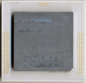
Compaq 21364 Alpha Prototype – 2002
The DEC Alpha was one of the fastest processors of the 1990’s. The original 21064, manufactured in CMOS, rivaled the fastest ECL processors and blew away most everything else. Clock speeds were 150-200MHz (eventually hitting 275MHz) at a time when a standard Intel PC was hitting 66MHz, at the very top end. It was manufactured on a 0.75u process using 1.68 million transistors. The Alpha was a 64-bit RISC design, at a time when 16-bit computing was still rather common. This gave the architecture a good chance at success and a long life.
The 21064 was followed by the 21164 in 1995 with speeds up to 333MHz on a 0.5u process, now using 9.3million transistors. It added an on die secondary cache (called the Scache) of 96KB as well as 8KB instruction and Data caches. These accounted for 7.2 million transistors; the processor core itself was only around 2.1 million, a small increase over the 21064. At the time the main competition was the Pentium Pro, the HP PA8800 and the MIPS R10000. Improved versions were made by both DEC and Samsung, increasing clock speeds to 666MHz by 1998.
In 1996 DEC released the next in the series, the 21264. The 21264 dropped the secondary cache from the die, and implemented it off chip (now called a Bcache). The level 1 caches were increased to 64KB each for instruction and data resulting in a transistor count rise to 15.2 million, 9.2 million of which were for the cache, and the branch prediction tables. Frequency eventually reached 1.33GHz on models fab’d by IBM. However the end of the Alpha had already begun. DEC was purchased by Compaq in 1998, in the midst of the development of the enhanced 21264A. Compaq was an Intel customer, and Intel was developing something special to compete with the Alpha.
Read More »
September 14th, 2013 ~ by admin
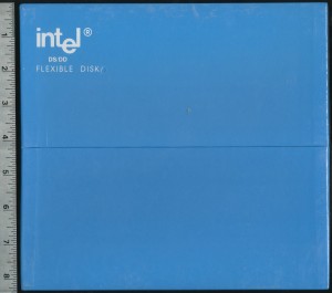
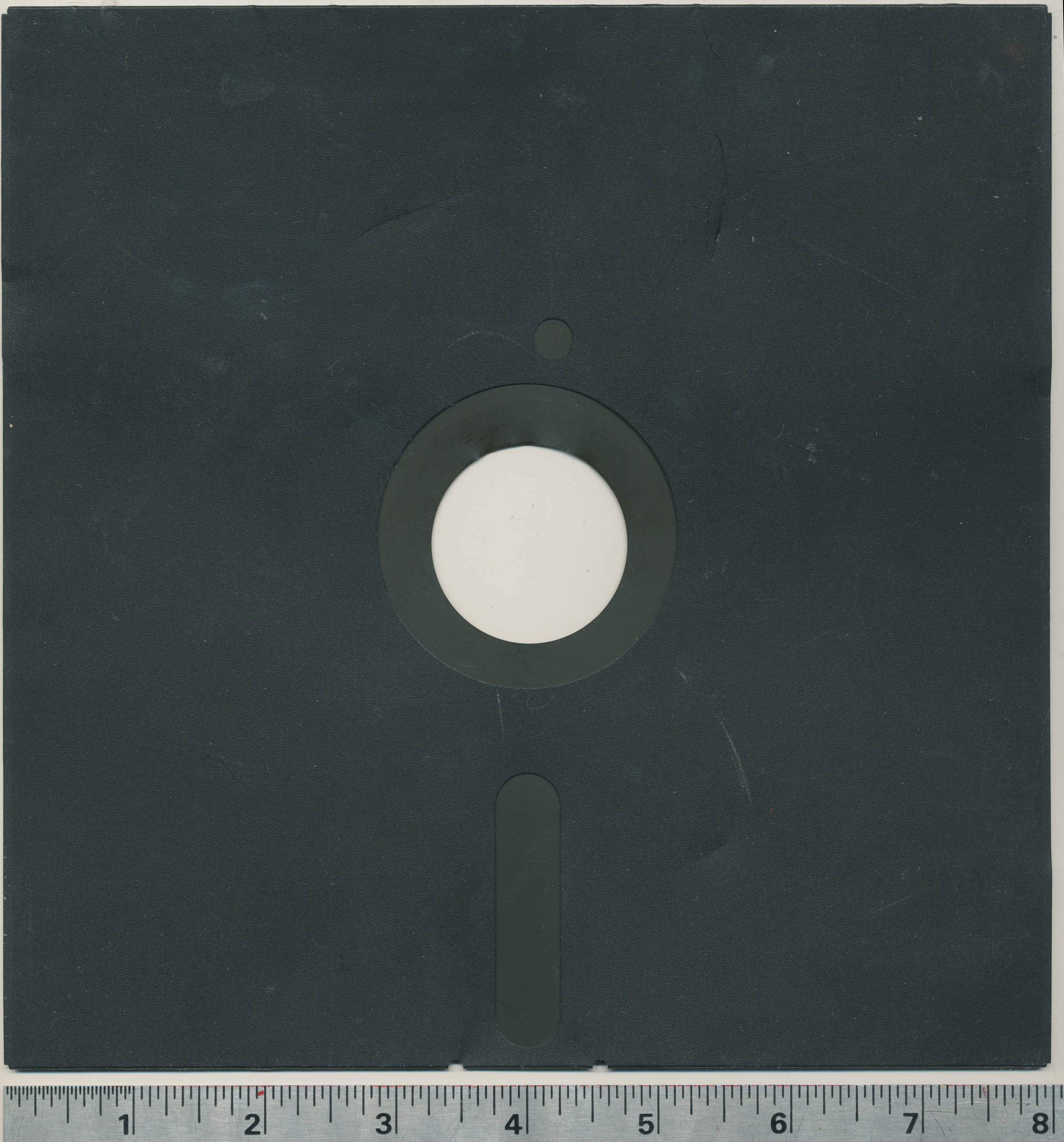
Intel 8″ Floppy Disks (10 Pack) – Minimalist Packaging ahead of its time. 1.2MB
The original floppy disk was introduced by IBM in 1971 as a way to serve updated microcode to their clients mainframes. Each disk could hold around 80KB. By 1977 the DSDD (Double Sided, Double Density) 8 Inch disk was released which held 1.2MB of data. They were officially known as a ‘Flexible Disk’ but floppy disk rapidly became what people referred to them as. Intel marketed and sold them as well as many other manufacturers. Intel accepted code for MaskROM based processors, on 8 inch floppy, tape, and a variety of other formats in the 1970’s. Certainly 1.2MB was a great plenty of storage for the 1-8KB of ROM most microcontrollers and MaskROMs supported in that era.
In 1978 a ‘consumer’ version of the floppy was released, in a more friendly size, but lower capacity. This was the 360KB 5.25″ disk that was eventually made famous by the IBM PC, TRS-80, Apple. and about every other computer of the late 1970’s and early 1980’s. 
Floppy disks continued to evolve into the late 1990’s trying to compete with the CD-ROM, with capacities eventually hitting 240MB with the LS-240 Laser Servo drive. In the early 21st century companies, largely led by Apple, began to delete the floppy from their computer line up, causing quite a stir. However, users quickly realized that contrary to popular belief, the floppy really wasn’t used much. Ultimately the use of the floppy, and the CD have been replaced with the USB Flash Drive, and in many ways, cloud computing.
September 3rd, 2013 ~ by admin

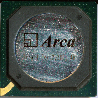
Arca-1 Rev2 166Mhz Processor – Late 2001
China is generally seen as where devices are made or assembled, rather then where they are designed or invented, certainly in the computer world. In 2001 a Chinese Gov’t funded venture known as ARCA Technologies changed that. ARCA (Advanced RISC Computer Architecture) designed and released a completely new processor known as the Arca-1. At the time there were two design houses working to create China’s first CPU. Arca, and BLX. BLX made the Godson series of processors which are MIPS32 and MIPS64 implementations. Arca, took a different approach. Not only did they seek to make an indigenous design, but they wanted to do so with their own Instruction Set Architecture (ISA).
The ArcaISA is, of course, RISC based, it contains 80 instructions, with each instruction consisting of up to 3 operands, and contains 32 general purpose registers. The original Arca-1 design is made on a 0.25 micron process (by which foundry is unclear, BLX used ST) with a 5-stage pipeline and drawing 1.2W at a clock speed of 166MHz. It contained separate 32 way associative 8K caches for Instruction and Data. The Arca also includes a DSP unit that has a pair of multiply/Accumulate Units (MACs) as well as basic SIMD support for media acceleration (including hardware MPEG2). Not exactly impressive for 2001, but not bad for a first release. However there was more to come.
Read More »
August 31st, 2013 ~ by admin
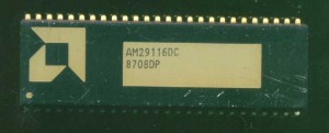
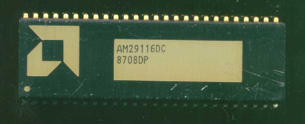
AMD AM29116DC – 1987 10MHz
In 1980 there was not yet a clear winning architecture for microprocessors. Many of the companies of the 1970’s were still churning out designs, hoping for design wins. Intel had yet to become a dominating force, though their 8086 line was becoming popular. AMD was one of the innovators of the time. Now known for their x86 processor, AMD made many other designs that were very successful.
In 1980 AMD was already making 2 16-bit class processors. They were a second source for the Intel 8086 (8/16 bit) as well as the primary second source for the Zilog Z8000 processor. They soon would pick up manufacturing demand for the Intel MCS-51 line as well. This was not enough for AMD, they sought to design a 16-bit microprocessor that would excel at high speed control applications (such as telecom and disk controllers). Thus began one of the most ambitious and complex designs of the time. In order to meet their performance goals the design had to be done in ECL, on a bipolar process, this is a bit more complicated for a large device then a NMOS part, mainly due to its power requirements and heat.
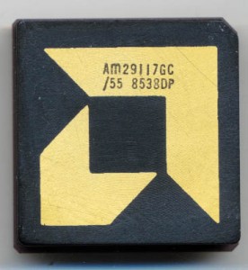
AMD AM29117GC – 1985 – Dual port version
In 1981 AMD announced the Am29116 microprogrammed 16-bit processor. It was made on a 2 micron process and contained 2500 effective gates (~14,000 transistors, 50mm2 die area). Max speed was 10 MHz. Samples were available starting in early 1982. The target competition was not the 8086 or Z8000 but The DEC T-11 ‘Tiny’ processor, which was made in NMOS and ran at 2.5MHz. The Am29116 is technically a bit-slice processor, like AMD’s wildly successful 2901 processor but adds a bit more functionality including instruction for bit manipulation, CRC generation, as well as a barrel shifter and an on chip scratch pad RAM (32x16bit). It has an accumulator, ALU, status register, and instruction latching/decoding for the 167 instructions. What the 29116 lacks is a PC (Program Counter). Program sequencing is handed by external logic, either custom, or using AMD 29112 microprogram sequencers. It is the job of the sequencer to feed instructions to the 291116, handled jumps, calls, returns, and memory accesses. This puts the 29116 somewhere between the basic 2901 and a full featured processor like the Z8000. AMD also produced the 29117 which added a second 16-bit port, resulting in a dedicated input port (D) and a dedicated output port (Y), whereas the 29116 had a single I/O port. This allowed for faster processing where data could be read and written simultaneously. The 29117 was available in a PGA68 package (16 more pins then the DIP52 of the 29116)
Read More »
August 8th, 2013 ~ by admin
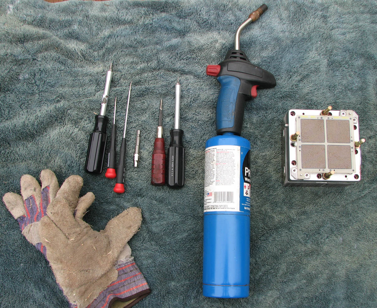
The IBM POWER4 was released in 2001. It was a 1.1-1.9GHz dual core processor widely used in IBM’s server line including the RS/6000 and AS/400. It can be commonly found as a single chip dual core, but also as a large MCM containing 4 POWER4 dies. These MCMs include a very large and heavy aluminium heatsink attached to a solid copper housing. The complete unit weighs in at a hefty 3kg. The heatsink and housing can be removed revealing a 230 gram MCM (with its small heat spreaders).

To disassemble one of these you will need a variety of tools. A 4 mm socket, hex bits (2.5, 3 and 4mm), T8 torx bit , a medium flat tip screw driver, gloves and a good heat source (I use a propane torch)
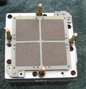
First remove the 4 T8 torx screws that hold the interposer to the module. It gets in the way and can melt easily. Also remove the 8 3mm screws around the perimeter. These hold the aluminium heatsink to the copper housing.
Read More »
August 3rd, 2013 ~ by admin

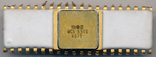
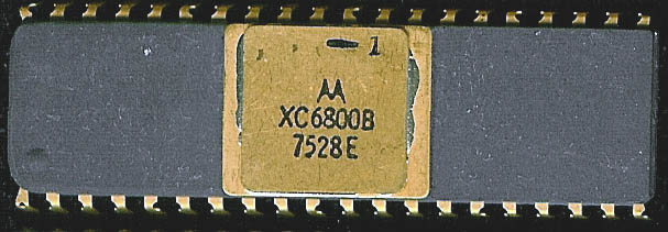
MOS MCS6501 – November 1975
One of the classic stories of the 1970’s microprocessor boom times was that of MOS Technologies at WESCON (Western Electronics Show and Convention) on September 16th 1975 in San Francisco. MOS Technology was a newcomer to microprocessors. They had with them two brand new processor design, the MCS6501 and the MCS6502 which they hoped to sell on the floor at Wescon, for $20 and $25 each. However Wescon forbid sales on the convention floor, so quick thinking by MOS Technologies Chuck Peddle directed people to a hotel room, where “the beer was free and chips were $25.” In the room were jars of 6501 and 6502 processors, to give them impression that these were in full production. In reality the bottoms of the jars were filled with defective parts. It was no matter, the 6500 series was a huge hit, led largely by its availability, low price and marketing to everyone (not just ‘big corporate users’). The 6500, and specifically the 6501 have an interesting story leading up to that fateful day at WESCON.
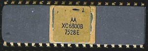
Motorola XC6800B – July 1975 – Pre-production part, not something MOS bothered with.
It begins at Motorola, where Chuck Peddle, Bill Mensch and several others were employed in the early 1970’s design the MC6800 processor and its peripherals. The 6800 was not a bad design, it was however, very expensive, a development board for it costing over $300. Chuck worked largely as the 6800 system architect, ensuring all the ICs worked well together and were what was needed to meet customers needs. He attended many calls to potential clients and noted that many were turned off by one thing, price. With that in mind he sought out to build a lower cost version of the 6800 using some of the newer processes available (specifically depletion mode NMOS vs the enhancement mode of the 6800). Motorola management wouldn’t hear it, they wanted nothing to do with a lower cost processor available to the masses. And with that, Chuck, Bill and over half the 6800 team left.
Read More »
July 26th, 2013 ~ by admin
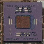
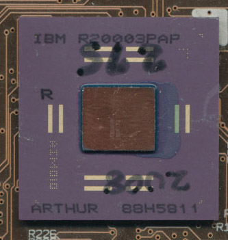
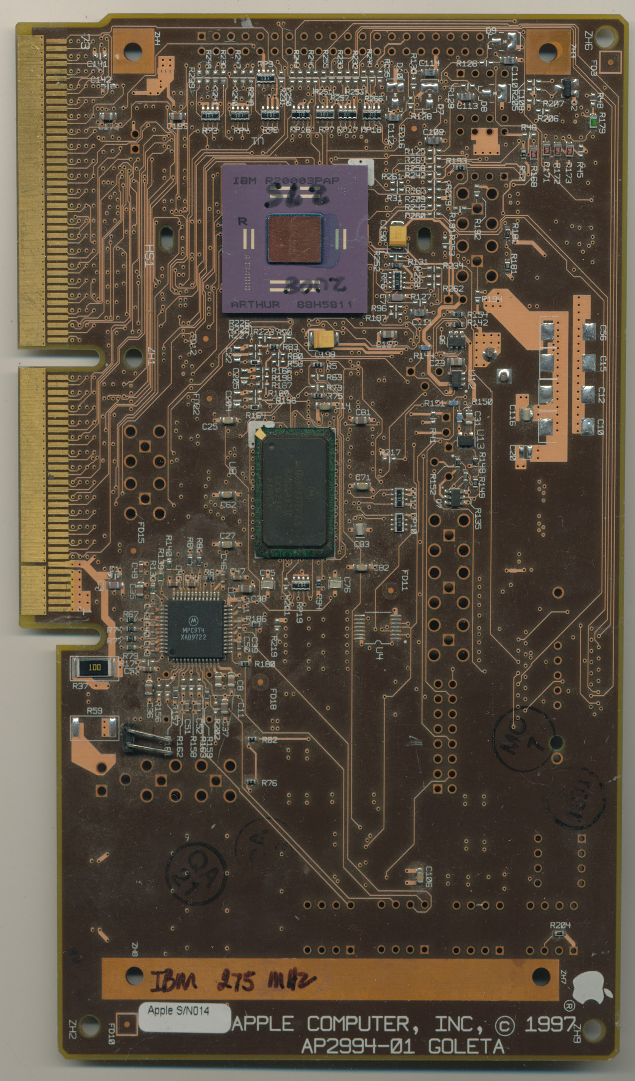
IBM Arthur Processor – 1997
By 1997 the PowerPC 604e was getting a bit dated. Apple needed an updated faster processor for their new computers and IBM and Motorola needed a new processor to sell to Apple. The PowerPC 750 was an evolution of the 604e and became the core of Apple’s various G3 systems.
In early 1997 Apple , IBM, and Motorola (together known as the AIM Alliance) were working on what would become the PowerPC 750. It’s code name? The Arthur. Apparently someone at IBM or Motorola had a liking for Sherlock Holmes as the 745 was codenamed Conan and the 755 Doyle, after Sir Arthur Conan Doyle, writer of Sherlock Holmes. This particular part is date coded R20003PAP which means it was made in mid-May of 1997, 6 months before the G3 and PowerPC 750 were officially released.
The card the Arthur processor (hand labeled 300Mhz) resides on is an Apple Prototype known as the Goleta. The Goleta was one of the first Apple G3 products. It was to be used in the PowerMac 9700 aka the PowerExpress which was to be a 6 slot G3 PowerMac running at 275MHz.
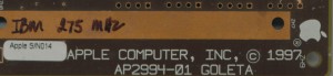
Apple Goleta G3 Prototype – Click here to see the full card.
It never made it past the prototype stage. The card is labeled as serial #014 making it a very early prototype, though how many total were made is not known. The card may have been used at Apple for testing other deigns as well and certainly was a test bench for the new 750 PowerPC Processor. This was a chaotic time for Apple as they were struggling to pull out of near bankruptcy. Steve Jobs had only just returned to the company and radically changed what Apple was doing, and what they were not doing (making money).


