September 16th, 2012 ~ by admin

MME U552D – Plastic 1702
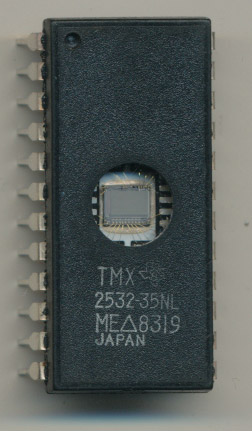
Today’s EPROM is a very rare early prototype from MME (VEB MikroElektronik “Karl Marx” Erfurt ). Part of the East German state-owned electronics business. MME (and their predecessor FWE) made clones of Intel 1702, 2708-2764 EPROMs as well as many processors. These were all unlicensed, reverse engineered, or copied via industrial espionage since this was all before the end of the USSR, and the technology blockade put in place to ‘prevent’ Eastern Europe from using Western technologies. This particular U552D is a clone of an Intel 1702A, however, it is made in a plastic package (with what appears to be a actual quartz window). A very unusual package that was used in Soviet devices mainly and very rarely in the west.
The only western EPROM I have found in plastic is a prototype TMX2532-35NL from Texas Instruments (thus the TMX prefix).
However, the MME U552D actually has the window glued to the top of the plastic package, rather then integrated into it like the TI, and the Soviet designs.
September 6th, 2012 ~ by admin
Back in 2010 we did a write up on the many processors in each iPhone for each version through the iPhone 4. Since then Apple has released the iPhone 4 (CDMA) and the mid-cycle refresh iPhone 4S. Seeing as the iPhone 5 should be released on September 12th here is a quick update to bring our table up to date.
CPUs by function and generation of iPhone:
| Function |
2G |
3G |
3GS |
4 |
4-CDMA |
4S |
| App Processor |
Samsung S3C6400 400-412MHz ARM1176JZ |
Samsung S3C6400 400-412MHz ARM1176JZ |
Samsung S5PC100 600MHZ ARM Cortex A8 |
Apple A4 800MHz ARM Cortex A8 |
Apple A4 800MHz ARM Cortex A8 |
Apple A5 900Mhz Dual core ARM Cortex-A9 |
| Baseband |
S-GOLD2 ARM926EJ-S <200MHz |
Infineon X-Gold 608 ARM926 312MHz + ARM7TDMI-S |
Infineon X-Gold 608 ARM926 312MHz + ARM7TDMI-S |
X-Gold 618 ARM1176 416MHz |
Qualcomm MDM6600 ARM1136JS 512MHz |
Qualcomm MDM6610 ARM1136JS 512MHz |
| GPS |
NA |
Infineon HammerHead II |
Infineon HammerHead II |
BCM4750 (no CPU core) |
see above |
see above |
| Bluetooth |
BlueCore XA-RISC |
BlueCore XA-RISC |
BCM4325 (2 CPU cores) |
BCM4329 (2 CPU cores) |
BCM4329 (2 CPU Cores) |
BCM4330ARM Cortex-M3 + Bluetooth CPU |
| Wifi |
Marvell 88W8686 Feroceon ARMv5 128MHz |
Marvell 88W8686 Feroceon ARMv5 128MHz |
see above |
see above |
see above |
see above |
| TouchScreen |
Multi-chip |
BCM5974 |
TI |
TI |
TI |
TI |
| OS |
Nucleus by Mentor Graphics |
Nucleus |
Nucleus |
ThreadX by ExpressLogic |
REX by Qualcomm |
REX by Qualcomm |
| Total Cores |
5 |
7 |
7 |
5 |
5 |
6 |
Apple iPhone 4 CDMA
The CDMA version of the iPhone 4 switched from an Infineon X-Gold baseband to a Qualcomm MDM6600 running a 512MHz ARM1136JS core. Interestingly this baseband supports GSM but due to antenna issues it is not implemented here. The Qualcomm Gobi, as it is known, also has integrated GPS, removing the need for the old Broadcom BCM4750. This sets the stage for the iPhone 4S.
Read More »
September 6th, 2012 ~ by admin
A Brief History
Long before the mess of Apple vs. Samsung (and seemingly everyone else), there was another famous company, with a patent in hand, that it seemed everyone was violating. The issue of Intellectual Property (IP), and its associated patents has long been an issue in the technology business, and certainly in the business of CPU’s. There are many many functions inside a CPU, different structures for handling instructions, memory access, cache algorithms, branch prediction etc. All of these are unique, intellectual property. It doesn’t matter if you implement them with a slightly different transistor structure, as long as the end product is relatively the same, there is the risk of violating a patent. Patents are tricky things, and litigating them can be very risky. You must balance the desire to keep competition from violating your IP, but at the same time minimize the risk that your patent is declared invalid. This is why most cases end up in an out of court settlement, usually via arbitration. Actual patent jury trials are fairly rare, as they are very expensive and very risky to all parties involved

Infringing?
In the early days (1970’s and early 1980’s) there was routine and widespread cross licensing in the industry. Many companies didn’t have the fab capacity to reliably meet demand (IBM wouldn’t purchase a device unless it was made by at least 2 companies for this very reason) so they would contract with other manufacturers to make their design. Having other companies manufacture your design, or compatible parts, also increased the market share of your architecture (8086, 68k etc). For years AMD made and licensed most everything Intel made, AMD also licensed various peripheral chips to Intel (notably the 9511/2 FPU). As the market grew larger, the competition increased, Intel (and others) began to have enough reliable fab capacity to safely single source devices. Meanwhile other companies continued to make compatible products, based on previous licensing. AMD notably made x86 CPU’s that ate into Intel’s market share. In the 1970’s Intel had cross license agreements with AMD, IBM, National, Texas Instruments, Mostek, Siemens, NEC and many others.
Read More »
August 30th, 2012 ~ by admin

z12 MCM Layout
“We are hitting the limits of physics in many cases” These words, spoken by an IBM engineer about the new zEnterprise EC15 mainframe do well to describe the processor that runs it. The z12, as we’ll refer to this processor, replaces the z196 as IBM’s top performer. The z196 ran at a slothly 5.2GHz, the fastest commercial processor in the world until now. The z12 runs at 5.5GHz and was designed to be clocked up to 6GHz. It is made on a 13layer 32 nm High-K process (the z196 was made on a 45nm process). This allowed a doubling of logic and cache density.
The EC12 is designed with single thread performance in mind. While many systems today focus on massive parallelism, and optimizing code for multi-threading, some tasks do not work well that way, data analytics, batch processing etc, are fundamentally serial processes, so less cores, and more speed per core is far more important. The z12 is based on a MCM (Multi-chip module) that contains 6 Processing Units (PUs) and 2 Storage Controllers (SC, which contain 196MB of L4 cache each) for a total of 8 dies on each MCM. Each PU contains 4, 5 or 6 active cores. The MCM is a 103-layer glass ceramic substrate (size is 96 x 96 mm) containing eight chip sites and 7356 land grid array (LGA) connections.

IBM zEC12 6-core PU – 2.75 Billion Transitors – 5.5GHz
Each PU chip has 2.75 billion transistors. Each one of the six cores has its own L1 cache with 64 KB for instructions and 96 KB for data. Next to each core resides its private L2 cache, with 1 MB for instructions and 1 MB for data respectively.
Read More »
August 29th, 2012 ~ by admin

Shugart SA400 Floppy Drive
The HP Input Output Blog has a nice write up on the floppy disk/drive. A very interesting read about a device many took for granted, and many of today’s generation did not ever get to experience. Many do not realize its humble beginnings, and the importance that Steve Jobs, ‘the bum in the lobby,’ played in the 5.25″ floppy becoming a standard. The 5.25″, holding twice what a 8″ floppy could, was developed by Shugart Associated in 1976. Shugart went on to become Seagate, known today for their hard drives. Hard drives that can store over 2 Terabytes of information. The original 5.25″ floppy? 160K, per side. An 8 inch? 80K a side. Interestingly enough, it was sometime before the Floppy Drive Controller (FDC) was integrated onto a single chip. Many original Shugarts used an Intel 8080 CPU for drive processing. The Commodore 64’s famous 1541 Floppy Drive ran its own 6502 type CPU, and was designed in such away you could actually load code directly to the floppy drive 6502. In the 1990’s attempts were made to increase the capacity, speed, and versatility of the floppy. Apple created a 2.88MB 3.5 inch floppy that never really caught on. There was the LS-120 drive which could use normal 1.44MB disks as well as special 120MB disks (was handy, but so few people had them, they had limited use). Ultimately, like most all technology the floppy has passed by the way side, today’s floppy is the USB Flash drive, holding many gigs of data for only a few dollars. And like the floppy, flash drives are used commonly for sneakernetting files around the office. Perhaps the mbile version of the floppy is the Micro-SD card, remember when Sony built a camera with a 1.44MB floppy drive built in? Not een large enough to store the picture from a cell phone camera today.
Head on over and check out the article, its a fascinating story….
August 16th, 2012 ~ by admin
 Yesterday Hans Camenzind passed away at the age of 78. Hans was a notable inventor of Swiss decent. Perhaps the most famous of all his inventions occurred in 1972 while working on a contract with Signetics he invented the 555 Timer chip, a simple oscillating IC that was inexpensive, and easy to build with. Now, even 40 years after its introduction, around a billion per year are still made, by dozens of companies around the world. The 555 Timer is often one of the very first IC’s electronics hobbyist begin experimenting with. Its applications are far reaching and while certainly not a CPU, its significance, and that of Camenzind, should not be forgotten.
The 555 Timer has of course been used in many many computers, notably in the Apple II computer as a joystick controller (558 Timer, which is a quad 555). Other uses include the IBM PC, Ataris, and many many more. In honor of Hans Camenzind, and the 555 Timer, go experiment with one and experience the joys of a device over 40 years old. Dont have one? They cost a whopping $0.95 at Sparkfun.
August 14th, 2012 ~ by admin
The Spacecraft CPU page has been updated, after a long gap. It now includes information of the recently landed Curiosity Lander, some new information on the 45 year old Voyager series as well as some on New Horizons, DAWN, and several others, so check it out.

BAE RAD750 Single Board Computers
The Curiosity (and Mars Reconnaissance Orbiter,) Run a BAE RAD750 @ 200MHz
July 28th, 2012 ~ by admin
While we don’t actively collect GPU’s, we do pick them up when they come along, rather then scrap them, and from time to time have been donated a handful of them. Here are a few that have been sitting on my desk that were donated. GPU’s are pretty impressive in their own right (with many having over 1 billion transistors now)

Nvidia NV43 ENG SAMPLE
The NV43 is the code name for the Geforce 6600. It was released in August 2004 (abut the time this Engineering Sample was made) and could be clocked at up to 525MHz. It was fab’d by TSMC on a 110nm process and contains 143 million transistors (about the same as a Pentium-M Dothan core).
Read More »
July 26th, 2012 ~ by admin
 Out of the annuls of history comes this interesting computer on eBay. PIXAR made around 300 of their Image computers during the late 1980s, hoping they would be a commercial success, as well as useful for their own render work. While they proved to be very good at what they did, they were a bit ahead of their time, and certainly out of the price range of most institutions. The first models started at $130,000 and the PII, as seen on eBay, was sold for $30,000. PIXAR began trying to sell their computers two months after Steve Jobs bought the company (formerly LucasFilm graphics division).
Each system ran 1, 2, or 4 CHAPs (CHAnnel Proceesors, RGBA). Each CHAP consisted of a board with 4 AMD 29116 16-bit bipolar bit slice microprocessors, running at 10MHz supported by 4 Logic Devices LMU17 16 x16 parallel multipliers.

AMD AM29116 16 bit microprocessor
Essentially the PIXAR Image Computer was a 1980s GPU, it required a separate SGI or Sun workstation to run.
September 29th, 2011 ~ by admin
Leaving on a trip so I dumped all the pending CPUs/EPROMs etc to a gallery.
There are litterally thousands of new CPU’s, EPROM’s, FPU’s, and some oddities.
They are sorted by manufacturer (technically brand)
You can view them in gallery form here:
https://www.cpushack.com/updated-museum-collection-photos/
You may also view them in raw directory form here:
https://www.cpushack.com/CPU_Photos2/
and a few that didnt make it into the gallery here:
https://www.cpushack.com/CPU_Photos/


