January 18th, 2019 ~ by admin

Part 4: Mini-Mainframe at Home: Benchmarks and Overclocking

Part 4 of the Story of a 6-CPU Server from 1997.  In this final section we will first explore (briefly) the theory of running a 6-CPU SMP system (with processors designed for 2 or 4 way) and then move to benchmark the system and overclock it.

For the background of the ALR 6×6 and Pentium Pro processors that form the basis of this project please see:

Previous Parts of the Series

Part 1: Mini-Mainframe at Home – Introduction
Part 2: Mini-Mainframe at Home: Installing a Modern OS
Part 3: Mini-Mainframe at Home: The ALR 6×6 Hardware and BIOS

Features of the architecture and operation of the six CPU

So, as the server was originally shipped with six Pentium Pro “Black” processors, I decided to add six Pentium Pro “Gold” processors with a frequency of 200 MHz and a 256 KB L2 cache for contrast. Such a volume is just four times smaller, and at the same time it will be interesting to check the effect of the cache in such a volume: six megabytes versus one and a half.  But before starting the tests, I will focus on the principle of interaction of six processors in this system. To overcome the limitations of Intel on building a system with more than four processors, ALR engineers with the support of Unisys suggested using an inter-processor interaction scheme using arbitration:

The theory behind this architecture is as simple as it is powerful. Inside new six-way systems are two Tri-6 CPU cards, A and B (Figure 1). Each of these cards is an independent, three processor ready SMP bus, complete with all logic Active CPR processor protection, and auto-recovery technology built on each CPU card. These two Tri-6 CPU cards are then plugged into a 64-bit parity SMP bus. This design keeps the processors closely coupled, just like a parallel bus architecture, without the related heat and design problems. A separate four-way interleaved memory card is attached to the bus, supporting a sustained data bandwidth of 533-MB per second. This bandwidth is ample to support two full PCI buses as well as an EISA bus bridge.

To overcome the logical limitations of the Pentium Pro chip, six-way servers use a unique expanded bus arbitration configuration referred to as Dynamic Orchestration. The best way to understand how this system works is to compare it to a typical four-way SMP architecture. On a four-way system, bus arbitration is implemented in a “round robin” fashion. That is, each processor has equal rights to the bus, and access is handled in an orderly fashion. For example, if all processors needed access to the bus, CPU 0 would gain access first, followed by CPU 1, CPU 2, CPU 3, and then back to CPU 0. If CPU 2 was executing a cycle, and both CPU 3 and CPU 1 requested use of the bus, control would first pass to CPU 3, before cycling back to CPU 1.

For purposes of this four-way arbitration, processors are identified using the two-bit ID code. The six-way solution borrows this convention, with some important modifications. Within each Tri6 CPU card, individual processors are identified using the two-bit ID code. This yields four possible combinations, although only ID codes 0 through 2 are needed. A chip on each Tri6 card handles the arbitration, following the “round robin” scheme found in a four-way system. In this case, however, the fourth processor has been replaced by a sort of “phantom” processor that actually represents the other Tri6 card:

The figure above shows the six-processor scheme of the server board ALR Revolution 6×6 and its clones. Thanks to this approach, the appearance of 8, 10 and more processor systems has become possible.

Building a chessboard from various models of Pentium Pro, I thought that I could not find a larger processor. Even the 32-core AMD Threadripper 2990WX next to the Intel Pentium Pro does not seem so big.

However, The CPU Shack sent me this photo. On the left is the engineering version of the Xeon Gold 6142 on the LGA3647 socket, on the right another engineering version, but already the Intel Xeon’a Phi in the same LGA3647 version. As you can see, the story is back to square one and perhaps all subsequent processors will not be placed on the open palm of the hand. Although the processors in the performance of LGA2066 is still far from Intel Pentium Pro.

Overclocking 6 cores together and separately

Read More »

Posted in:
Boards and Systems

January 16th, 2019 ~ by admin

Part 3: Mini-Mainframe at Home: The ALR 6×6 Hardware and BIOS

Part 3 of The Story of a 6 CPU Server from 1997 – In this section we’ll learn about the hardware and BIOS that makes the ALR Revolution 6×6 with 6 Pentium Pro Processors work.

For the background of the ALR 6×6 and Pentium Pro processors that form the basis of this project please see:

Part 1: Mini-Mainframe at Home – Introduction
Part 2: Mini-Mainframe at Home: Installing a Modern OS

Exterior and Interior

The size of the case is quite large for the desktop (and it came with wheels, so probably not good  to have rolling about ones desk), but relatively compact for servers of this class. The height of the server is – 68 cm, width – 32 cm and depth – 58 cm. The weight of the server starts from 52 kg. I have a complete server kit, but the case is missing, because, due to its size and weight, the shipping to Belarus would be around $ 400, if not more, so the photos of the appearance were taken from the Internet.
Editor’s Note: The empty case is currently serving as a kitchen counter at the CPU Shack Museum.  Its really THAT big 

The first thing that catches the eye is the information touch! LCD display, the task of which is to display all the information about the status of the six processors, RAM, temperature, status of hard drives and other vital information. Today, such informative displays are the norm, but 21 years ago I even could not imagine that such a thing ever happened. The front of the case also has two compartments, the upper one under 5.25” devices, such as CD-ROM’s, the lower one opened access to the cage with SCSI drives. Behind you can see 14 expansion slots, a cooling system and a cage with power supplies.

To ensure the operation of  the server, two power supplies are needed, which are connected to a special board in the cage. The third power supply unit is a spare one in case of a single power supply failure. It is allowed to install four power supplies with the connection of two pairs to a pair of electrical outlets for complete duplication of all functions providing the server power.

Read More »

Posted in:
Boards and Systems

January 14th, 2019 ~ by admin

Part 2: Mini-Mainframe at Home: Installing a Modern OS

Part 2 of The Story of a 6 CPU Server from 1997 – In this section we’ll try to get a modern OS running on the ALR Revolution 6×6 with 6 Pentium Pro Processors.

For the background of the ALR 6×6 and Pentium Pro processors that form the basis of this project please see Part 1 of the project.

Part 2: Installing and Using an OS

Before you start installing the OS, you need to select the correct kernel of the operating system. To do this, at the initial stage of installation, press the F5 key.

In this case, we choose – MPS Multiprocessor PC, since the other options simply do not fit, since this server naturally does not support ACPI. In general, I will advise anyone who makes such experiments by choosing a more “modern” OS, which is older than the hardware itself – to turn off ACPI support in the BIOS (if present). This simple action will keep your nerves decent.

Windows Server 2003 R2 Enterprise Edition was installed and, as I wrote above, the system had one working CPU core.

Next, an attempt was made to install the operating system from the operating system itself using the update method, but at the initial stage the Windows Server 2003 Enterprise Edition installer warned me that a multiprocessor configuration not supported by the operating system was used.

But there are many ways to install the OS. Alternatively, I tried the OS “transfer method” with a known-workable SMP configuration. Taking the ASUS P2L97-DS motherboard on an Intel 440LX chipset with a pair of Intel Pentium-II with a frequency of 450 MHz, which should be deprived of a hardware error and chose the “MPS Multiprocessor PC” core, but the installation process did not start at the stage of copying the original files, reaching until installation on the hard disk. At this point, the system hung, not reaching the choice of the installation source. Much has been tried, loops, different drives and RAM, but all to no avail. At this point, a single Pentium-3 was also hanging on the Asus P3B-F motherboard (Intel 440BX chipset).

In the end, I decided to take another board with two SLOT 1 connectors – Asus P2B-D (Intel 440BX chipset) and a pair of Intel Pentium-III. OS Windows Server 2003 R2 Enterprise Edition was safely installed, it remains to transfer it to a six-processor server. As a result, having moved the necessary hard drive, I decided to do the first boot in “safe mode” in order to exclude the influence of different devices of both systems on each other, but as a result I received a BSOD.

Read More »

Posted in:
Boards and Systems

January 12th, 2019 ~ by admin

Part 1: Mini-Mainframe at Home: The Story of a 6-CPU Server from 1997

Introduction

This article/project is provided in cooperation with guest author max1024, hailing from Belarus. I have provided some minor edits/tweaks in the translation from Belarusian to English.

As part of this project, you will have a unique opportunity to learn about a mini mainframe worth more than a Ferrari, which had enormous power by the standards of 1997, as well as the intricacies of installing a more modern operating system on it and other interesting details. I think that to some readers, the bold name of the super server ALR Revolution 6×6 already says something, and it will be discussed in this article.

Pentium Pro Processor versions – Minus the Overdrive

Alone, it would be simply not realistic for me to translate everything I had planned, without the help of my comrades from the United States, Russia and Great Britain, this project would have remained a project on paper, but their invaluable help would make it possible for the planned and almost forty kilograms of net weight (nearly 90lbs) to go a long way, more than 11 thousand kilometers (6800 miles) for three separate packages. The total distance as a result of which all the parts came together was 30 thousand kilometers (18,000 miles)  – for reference, the circumference of the Earth is 40 thousand km. (~25,000 miles)),  So this work is partly their merit, for which I am immensely grateful.

Editors Note: This ALR 6×6 came from the CPU Shack Museum, having sat in my house for some years. While chatting to Maksim last year he mentioned he would like to find one, so it was clearly meant to be.  You can’t just ship an ALR 6×6 across the world to Belarus, at least not economically, so over several months I disassembled the entire server and shipped it in pieces to a mutual friend in Russia, who then forwarded it to Maksim in Belarus.

Connor Krukosky and his IBM z890

Before embarking on the initial part of the project, I’ll tell you that trying to understand Mainframes and supercomputers  , I realized one thing that it’s quite possible to assemble even a “mini” mainframe at home, as Connor Krukosky did, but also overclocking would be even more interesting.

Studying such computational supermachines, I decided to dwell on systems consisting of Pentium Pro processors, so by installing Windows compatible applications and benchmarks, one could see how much the performance went ahead over the decades. Ideally, of course, it would be nice to get Intel ASCI Red, but I decided to start with its mini version.

Read More »

Posted in:
Boards and Systems

December 29th, 2018 ~ by admin

The End is Near (of the year) – A Look Back at Y2K

AMD Y2Kids Career Day – K6-2 Custom Painted 

Think back 19 years, the year is 1999 and in just a few days the world is apparently coming to an end due to programmers of the 60’s and 70’s deciding to save precious memory and use 2-digits for the year instead of 4.  Or perhaps they just assumed that in 30-40 years we really wouldn’t be using the same systems. Either way the world (and by world we mean mainly the media) was prepared to go dark as everything technology driven ground to a halt as the clocks struck midnight.  Kids pondered if this would mean an extended holiday break, while parents wondered if they would still have a job, or money in their computer controlled checking account.

Thankfully (though perhaps looking back that is becoming murky to some) it was a complete non-even, life, and technology continued at a record pace. And who would want to miss it? The GHz war between AMD and Intel was neck and neck at the turn of the millennium, with AMD set to win it by a few days.  This was the age of the Pentium 3, the Athlon and the K6-2.  Technology was glamorous and some of its downsides seen today were relegated to sci fi movies.  AMD and other companies held job fairs to acquire new talent, and also hosted Career Days for younger kids to see what went on in the exciting tech industry.  This specially painted AMD K6-2 CPU was likely handed out during such an event, probably either in Austin, TX (where AMD had a large fab) or Santa Clara, CA.  Its a NTK made package with a AMD package # 26351, the standard from 1998-2000 and used for most all late K6-2 CPUs. The child who likely would have received this, probably a middle schooler at the time would now be around 30, who knows how such an event affected them but it would be neat if they ended up working at AMD (or Globalfoundries) or at the very least sing an AMD powered computer.

November 20th, 2018 ~ by admin

The CPU Shack Museum Goes to SC18 in Texas

Well, at least some of our processors did.  SC18 was the 30th annual International Conference for High Performance Computing, Networking, Storage, and Analysis, held in Dallas, TX.  Being as this was the 30th anniversary, organizers wanted to provide a look back over the past 30 years of the conference, as well as the past 30 years of High Performance Computing.  Earlier this year CPU Shack published an article covering a large amount of this history of Supercomputers.  The SC18 exhibit had an actual Cray-1B Supercomputer and many other interesting relics.  The CPU Shack Museum loaned a variety of processors, from a Processor Node from an Intel Paragon Super Computer, to POWER and SPARC processors, and even a GRAPE-6 processor.

Here are a few images of the conference.  The first two images (681 and 683) show the entrance area, entrance signage, the Cray-1B, and some of the display cabinets and diagrams on the wall above the cabinets showing year-by-year SCinet configurations.

SC18 Entrance w/ Display Cabinets

The Cray-1B was one of the first things the over 13,000 attendees got to see.

Cray-1B on the right

In the display cases were many vintage items from past conferences, as well as an assortment of processors.

SC18 Display Case: Spot the POWER, SPARCs,, GRAPE, and even a BlueGene compute node

The displays and processors generated many conversations, questions, and reminisces. There was over 350 exhibits from companies and Universities around the world.  The CPU Shack Museum is happy to have been able to help in a small way.

Posted in:
Museum News

October 12th, 2018 ~ by admin

Xilinx gets ARMed up for Free

Xilinx Virtex II Pro FPGAs from the 2000’s included embedded PowerPC processor cores.

Recently ARM announced they would be providing IP for the Cortex-M1 and M3 cores for free for users of Xilinx FPGA’s.  The Cortex-M1 and M3 are some of the most basic ARM cores, taking 12-25,000 gates for the Von Neumann architecture M1 and around 43,000 for the full up Harvard architecture M3 (with full ARM THUMB instruction set support).  Xilinx already offers FPGAs/SoCs with built in ARM cores, the SYNQ series is available with a variety of high end ARM cores such as the Cortex-A53 and the RF focused R5 core.  These obviously are fairly high gate county, and cost cores, where as the M1 and M3 cores are being provided without license, and without any royalties.  Drop in the IP into your FPGA design and go.

ARM and Xilinx say this is to meet the needs of their customers, who want to be able to use the same ARM architecture in their FPGA designs as in ASICs etc, and at the lowest investment in time and cost.  This certainly makes sense, having a free ARM core is better then a low cost ARM core, and removing the ‘paperwork’ hassle helps, but that’s probably not the only reason ARM is doing this, and doing it specifically for Xilinx.

There are a couple other things at play here, ARM Mx cores are basic RISC processors, used for when you just need to get some basic processing done, no frills, low power, and easy to use.  It turns out that’s a market that is now seeing some competition from the SiFive RISC-V core.  This is a basic, easy to use RISC core, that is synthesizable into ASICS, and FPGAs, and comes with a one time low cost license fee and no royalties.  Its being used by such heavyweights as Nvidia, and could threaten the Cortex-Mx domain, so it makes sense for ARM to offer, essentially their introductory processor core, for free, as a way to sway people to the ARM ecosystem.  But why Xilinx?

Perhaps Xilinx is just the start of ARM’s plans, Xilinx is one of the biggest providers of FPGAs in the world so certainly that will help keep people in the ARM. Xilinx infact, already has a drop-in 32-bit RISC processor core available to all their customers, the MicroBlaze and PicoBlaze, of their own design.  There are also drop in 80C186 cores, MCS-51 cores, the LEON SPARC core and many others. The other big name in FPGAs is Altera, a company that has competed with Xilinx for the better part of 30-years and was, in June of 2015 bought by none other then Intel.

Altera has had a close relationship with Intel since the 1980’s when Intel first started assisting Altera with fab’ing their PLDs.

This gave Altera greater access to Intel’s fab/engineering prowess, but also to all of Intel’s IP.  Is Intel going to offer free ARM cores on Altera FPGAs (the Stratix/Arria series does include hard Cortex-A9/A53 cores already)?  It seems unlikely that they would work to support their architectural competitor any more then they have to.  It is more likely that Intel would offer some form of 32-bit x86 processor core for their FPGAs.  Now x86 isn’t exactly known for low gate counts, but it is possible.  Currently softcore 8086 and 80186 processor (the Turbo86 and Turbo186) are 22,000 and 30,000 gates respectively, really a rounding error in FPGAs that now have millions of gates. More and more, FPGAs are becoming less FPGA like, and more ‘configurable processor’ like.

September 30th, 2018 ~ by admin

Peavey and the Motorola DSP56000

Motorola XSP56001ZL20 – 20.5MHz 1990

In 1985 Motorola was looking to create a DSP (Digital Signal Processor) line of processors to go with their very popular 68000 series of general purpose processors.  DSP’s are similar to a normal processor but, as their name implies, are designed to work on signals, versus data stored in memory.  Typical signal data is audio, video, RF (such as RADAR information) and anything else that comes in via an ADC.  These signals are processed via algorithm such as FFTs (Fast Fourier Transforms) to manipulate, change or analyse them.  In audio, this can be used for cleaning up an audio stream, adding effects to it, or even generating audio.

In the 1980’s the main single chip DSP competitors was the still in use TI TMS320 series. the ATT/WE DSP16 series, and some DSP’s from OKI/NEC.  When Motorola began work on what would become the DSP56000 they asked one of their long time customers, Peavey, what they would like to see in a DSP. Peavey is an audio equipment manufacturer, making such things as guitar amps and keyboards, so would have a good idea of what would be useful in a DSP designed for audio signals.

These were packaged in a ‘SLAM’ package. The contacts/traces were easily damaged by leaking batteries.

The DSP5600 is a 24-bit processor made on a 1.5u HCMOS process with around 150,000 transistors.  24-bits were selected as that was ideal for audio sampling at the time (and most ADS/DACs at the time max’d out at 20-bits of resolution anyways.  These DSP’s had a 3-stage pipeline and ran at 20.5MHz, 27MHz and 33MHz.  This provided around 10.25 MIPS of performance (at 20.5MHz).  They were a fixed point (no floating point support in hardware) design, which was adequate at the time.  A total of 62-instructions were provided.

The DSP56001 is identical to the DSP56000 except that it has 512×24-bits of on-chip program
RAM instead of 3.75K of program ROM and a 32×24-bit bootstrap ROM for loading the program RAM.  This is the version that became most popular.  Peavey used the 560001 (3 of them actually) to power the DPM3 SE keyboard back in 1990.  Recently J. Acorn, from Crasno Electronics in Canada sent The CPU Shack Museum an e-mail inquiring if I had a few of these now obsolete 56001 DSPs spare, to rebuild some dead Peavey keyboards.   As a Museum, I not only like to collect and present vintage IC’s but also regularly help people with project such as this, and have thousands of CPU’s sitting around that have been acquired through the years (really its a bit crazy how much I have collected lol).  Mr. Acorn needed 2 of these DSPs to replace ones destroyed by a leaking battery in a keyboard, and two is exactly what I had spare.  I dug them out, packaged them, and off to Canada they went.  The result?  A restored and working Peavey keyboard.  You can read about the restoration process on Crasno’s site.

The 56000 series continued to be made by Motorola (and then Freescale) up until 2012 when it was announced it would be discontinued as a standalone product.  The 56000 series cores though live on, inside of other Freescale (now NXP) products.


Posted in:
CPU of the Day

August 25th, 2018 ~ by admin

CPU of the Day: FOCUS on 32-bits

1983 HP FOCUS Board set – Pre FPU. Top left: Memory. Top Right: I/O and CPU bottom center

The year is 1981, Intel is making the 8/16-bit 8086/8088, and Motorola has released the 16/32-bit 68000 processor to much fanfare.  Motorola marketed this as the first 32-bit processor, but while it supports 32-bit instructions/data it does so with a 16-bit ALU.  HP, always used the MC68000 in their 9000 Series 200 line of computers, providing rather good performance for 1981. But this was the 1980’s and HP wasn’t satisfied with good, they wanted more, they wanted to implement a full 32-bit computer on something less then the 5,000 IC’s typically used to implement one at that time.  This meant making a processor like nothing else before, something with more then the 68,000 transistors of the MC68000 or even the 134,000 transistors of the new i286 Intel had announced.  What HP made is simply remarkable, in 1981 they announced the HP 9000 Series 500 computers, powered by an all new fully 32-bit processor called the FOCUS.  FOCUS was made on HP’s high density NMOS-III process, a 1.5u process, and used 450,000 transistors.  Thats 450,000 transistors on a single 40.8mm2 piece of 1.5u silicon in 1981, a smaller die than the Intel 286.

Read More »

Tags:
, ,

Posted in:
CPU of the Day

August 15th, 2018 ~ by admin

CPU of the Day: The 61 Knights of the Intel Xeon Phi

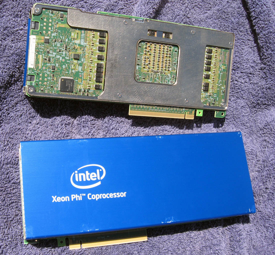
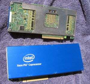
Xeon Phi – Knights Corner – Engineering Sample

In June of 2013, 20 years after the release of the Intel Pentium Processor, Intel released a new processor, technically a co-processor that Intel referred to as a MIC (Many Integrated Core).  It was branded as a Xeon, specifically the Xeon Phi 7000 series but at its core, it was nothing like a Xeon of 2013.  Code named Knights Corner, it built on the Knights Ferry.  Knights Ferry used many Larrabee GPGPU cores and was not designed as a commercial product.  Knights Corner , however, was, and to do so, Intel stuck with an architecture that customers were very familiar with, x86.  The Knights Corner integrated 61 Pentium P54CS cores onto a single chip.  The original Pentium P54CS was made on a 0.35u process and topped out at 200MHz.  They included 16K of L1 cache on die, and typically 256-512K of L2 Cache off chip.  The implementation of the Pentium on the Phi gets a bit of an upgrade.  The cores are made on a 22nm process (16 times smaller) and clocked at up to 1.2GHz.  L1 cache has been increased to 64K per core (32K Instruction  32K Data).  L2 cache remains at 512K

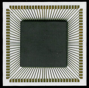
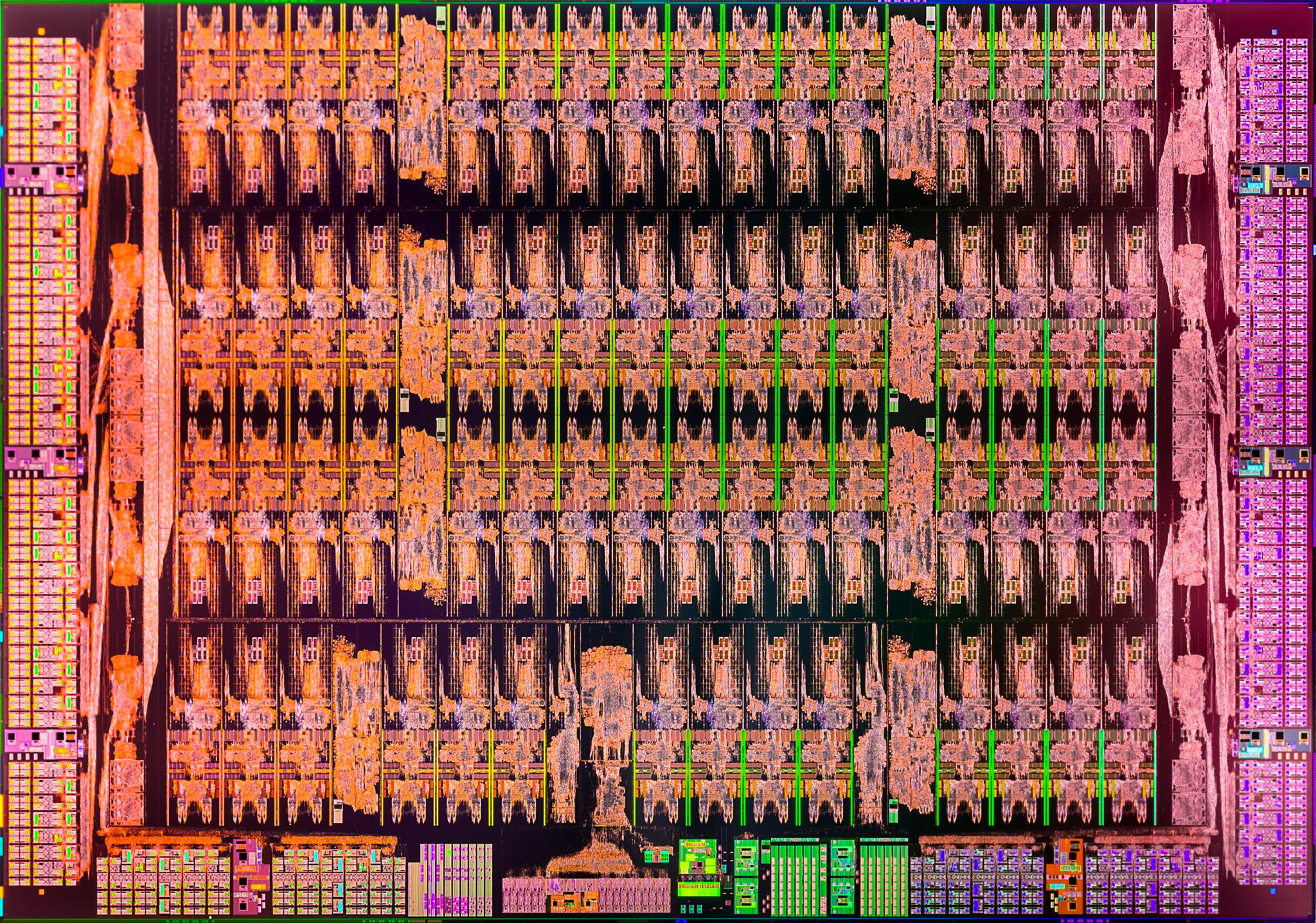
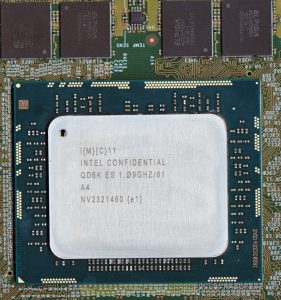
Knights Corner Die. – 62 Cores – 8 GDDR5 Memory Controllers

per core, but at 22nm, integrating all 30.5MB of cache on the same die becomes relatively easy.  The biggest change to the cores is adding support for 64 bit instructions, as well as adding a new execution unit called the VPU. This VPU (Vector Processing Unit) has its own 512-bit wide SIMD instruction set, integer support, Fused Multiply/Add, and other advanced features that are more commonly found in GPU’s. The VPU is the result of Intel’s work with Larrabee, the precursor to Knights Corner.  Interestingly MMX/SSE are not supported by the cores natively, this is handled in software (using virtualization) and leveraging the VPU included with the 61x Pentium Cores.  With the VPU, each core has 4 execution units (VPU, FXU, and 2 x Integer units). This allows the cores to support 4-way multi-threading; in practice, 2 threads are most common as 2 execution units are usually tied up calculating memory addresses.

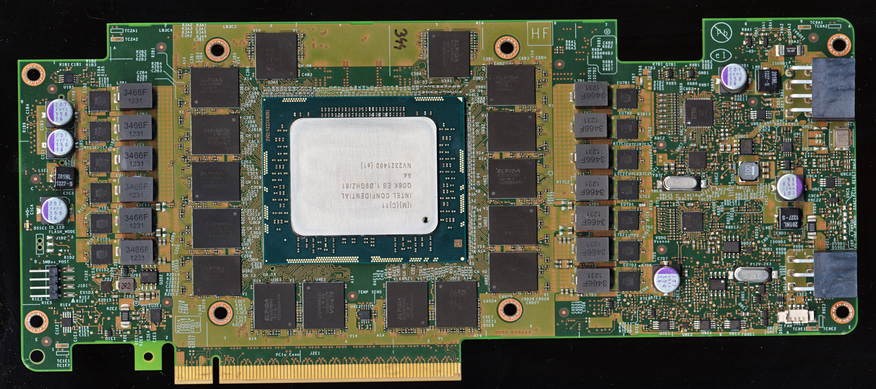
Knights Corner Sample – This is a 1.09GHz part while production versions were bumped to 1.1GHz – Elpida 2Gbit GDDR5 RAM chips surround the core.

For some reason Intel was very vague about information on die sizes/transistor count on the Phi.  Many sources claim 350mm2 die with 5 Billion transistors.  Taking apart a Phi shows that the die is actually much larger.  In fact the Xeon Phi die is 705mm2 and has 5.1 Billion transistors.  A 22nm Haswell Xeon with 18 cores has a die area of 622mm2 containing 5.6 Billion transistors. This means the Xeon Phi die wasn’t the most efficient is its use of space, likely due to the amount of room needed for the very large rings used to connect all the cores.  Looking at the die you can also see a lot of unused space.   There are actually 62 cores per die (with only 61 used max.)  This means 31MB of L2 cache which at 6 transistors per cell (bit) accounts for 1.5 Billion of the transistors.  L1 Cache is 64K per core so another 190 Million transistors there.  That leaves the bulk of the die for the cores, memory controllers, and the 3 interprocessor communication rings that handle communication between cores, MC’s (8 GDDR5 Memory Controllers per die), and the outside world.

Each Xeon Phi board includes the processor, as well as 6-16GB of GDDR5 Memory (8GB on the Engineering Sample here).  Memory is handled by 32 Elpida EDW2032BBBG-6 2Gbit GDDR5 6 Gbps chips. This gives the card is 352 Gbps memory bandwidth and 1 TFLOPS of computing performance.  All in a PCI-E car that dissipates around 300W.   Card/System management is provided by a NXP LPC2365FBD100 72MHz ARM7TDMI processor.

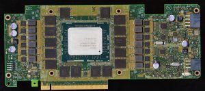
Knights Corner Xeon Phi with cooler removed. 16x 2Gbit GDDR5 (+16 on the back)

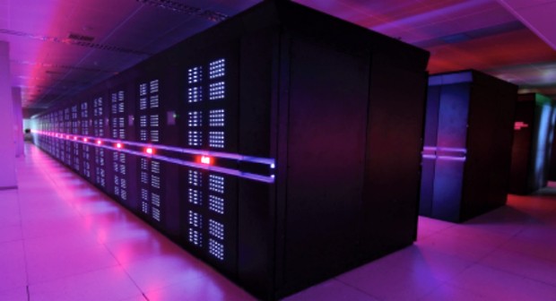
In January of 2013 the Texas Advanced Computing Center in Austin, TX announced the Stampede Supercomputer, the first large scale deployment of Xeon Phi Processors.  It used 6880 of them in its 6400 compute nodes and could hit nearly 10PFLOPS of performance. In June of 2013 the Chinese supercomputer Tianhe-2 became the fastest supercomputer in the world, a title it held until the end of 2015.  It was powered by 32,000 Intel Xeon E5-2692 2.2GHz 12C Ivy Bridge processors and a massive 48,000 Xeon Phi co-processors resulting in over 33PFLOPs.

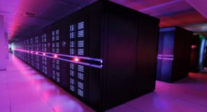
Tianhe 2 Super Computer with 48,000 Knights Corner Processors.

Intel made a successor to Knights Corner, known as Knights Landing, that was based on the Atom core, but then began to wind down the project.   Avinash Sodani, chief architect of the Knights Landing chip took a job at Cavium Networks (who make multicore MIPS networking processors), and Intel then hired Raja Koduri, the chief architect of AMD’s GPU processors.  Intel’s future seems to be one based on Xeon, and GPU’s.

Like the Knights of old, the the Xeon Phi has been passed up by other technologies, certainly still useful, but destined to the halls of museums and history books.  It came, and it conquered the Top500 Supercomputer list, and then quietly fades away.  On July 27th Intel quietly announced the discontinuation of the Xeon Phi line, with last orders accepted the end of this August (2018).