July 23rd, 2018 ~ by admin

A Sampling of Sample Processors

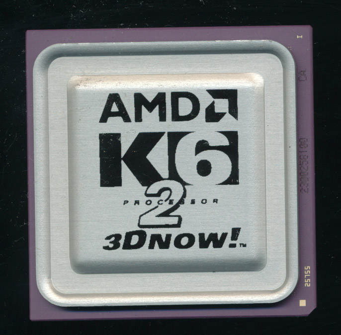
AMD K6-2 Marketing Sample

During the development of most any given processor many chips are produced before it is released for commercial use.  These pre-production chips serve a wide variety of purposes in the design and debugging of the processor to ensure that the final CPU work well, sells well, and is compatible with all the vendors parts (motherboards, cooling solutions, power supplies, etc).  These chips are generally referred to as samples, and there is several types of them.  We’ll use Intel/AMD as the main examples but most all processor companies work in similar ways.

When a processor design is first being developed, the package for it is also often being developed as well, what will the new processors silicon die reside in?  How many pins? How will it dissipate heat?  This type of testing is often handled with Mechanical Samples.  Mechanical Samples are exactly as they sound, they test the mechanical aspects of the processor, the physical fit of it.  THese are often sent to board/socket manufacturers to ensure the processor will fit in sockets/boards, and with the automated equipment used to build systems.  Cooling solution companies may also receive these to test how a heatsink fits on the CPU. Mechanical samples may not contain a die at all, or may be chips that were tested as bad, or simply just untested chips (Intel used a lot of untested Mechanical Samples in their educational kits).

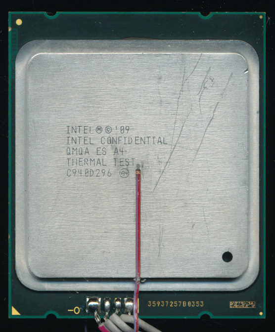
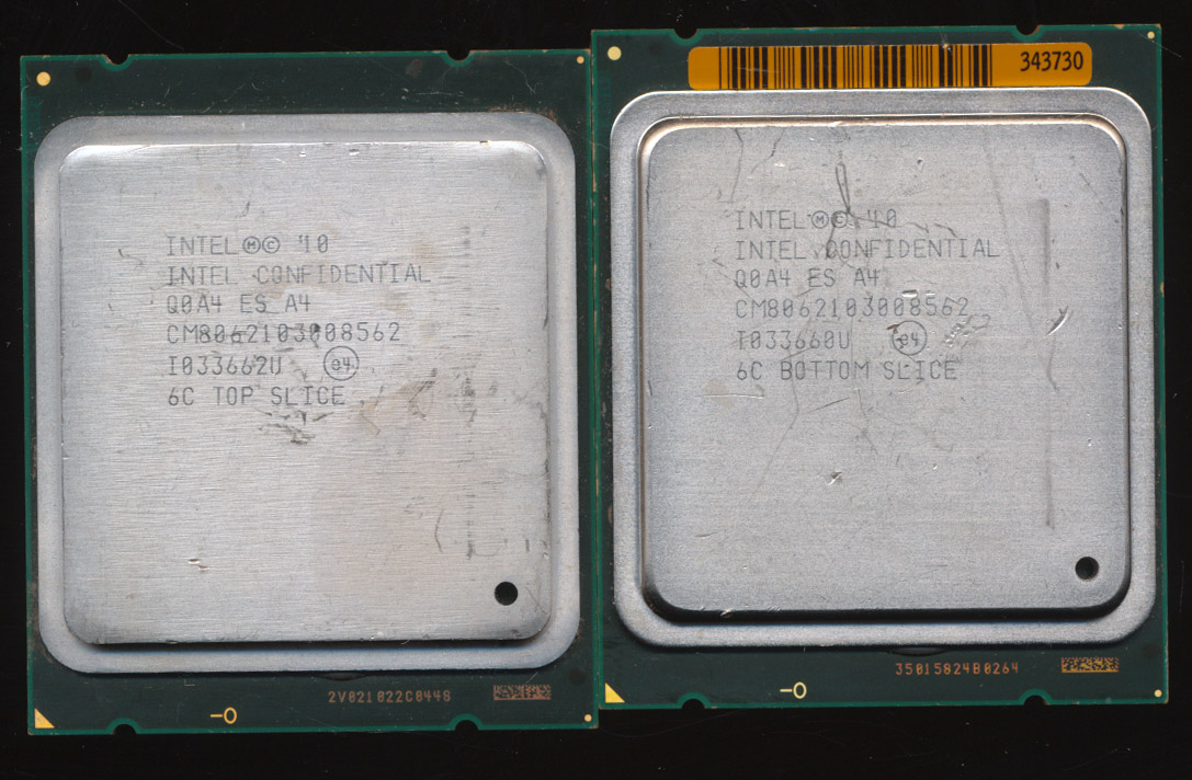
Thermal Sample for the LGA2011 Sandy Bridge Xeon

The next samples typically made are Electrical/Thermal Samples.  These again do not have an actually processor die in them, but electrically do work.  Electrical/Thermal samples are used to test the power draw and heat dissipation of a processor.  They often use a daisy chain transistor design, which serves to draw/dissipate power.  If a processor is expected to dissipate 135W of heat, a Thermal sample can be made to draw/dissipate exactly that.  These can test the the power supplies on motherboards, as well as the heat dissipation abilities of cooling solutions.  Some Thermal Samples have a temperature sensor added directly to the package to help see what temps they achieve.  Electrical Samples and Thermal Samples could also be used as purely Mechanical Samples too, and this is sometimes seen marked on the sample.

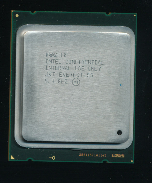
The first samples made that actually contain a functioning processor die are Engineering Samples.  Engineering Samples (also known as ES) are the most well known samples.  Overclockers often like to find ES CPUs as they will often allow for easier overclocking due to some not having locked in speed (multiplier locked).  Engineering Sample CPUs themselves come in several types as well.  Usually the first run is known as ES1, these can be thought of as an ‘Alpha’ version.  They are very likely to be buggy, and rarely run at the same speed as a production chip would.  These exist to test the overall processor design, or some subset of it.  Some are made to test just one part of the CPU, for example , the memory controller, or the cache.  Later versions of

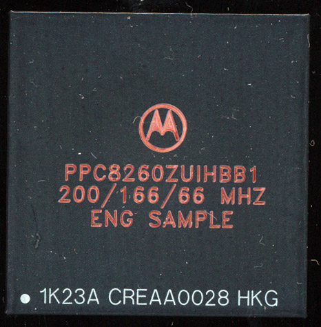
Motorola PowerPC 8260 Engineering Sample (note the PPC prefix)

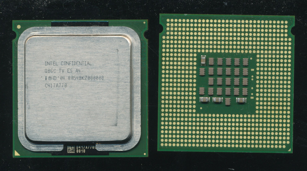
Engineering Samples are often called ‘ES2.’ These processors are getting closer to final production and are a lot less buggy, these would be considered ‘Beta’ Samples.  Most of the time these are quite usable chips, and often are very similar in clock speed/features to a production processor.   Intel denoted these chips with a Q-spec (such as QBGC) rather then production processor having an S-spec (such as SL5G8).  AMD typically uses part numbers starting with ‘1’ for ES1 CPUs and ‘2’ for ES2 CPUs. (such as Opterons 1S160805L4BGC or 2S16….).  Other companies have similar methodologies.  Motorola (Freescale) used the PPC prefix for most ES CPUs and Texas Instruments uses ‘TMP’ (not to be confused with Toshiba who also uses the TMP pre-fix, but for processors in general). Once a company is fairly confident a design is ready for release one final version is made.

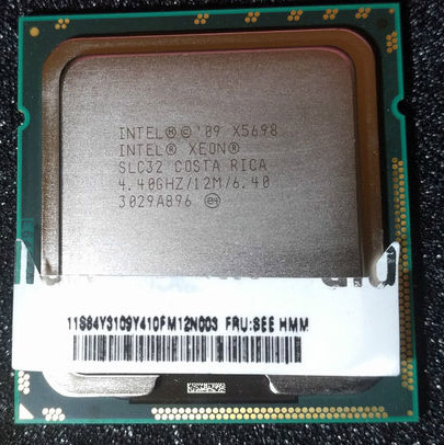
These are known as Qualification Samples (QS).  QS processors almost always have a one to one equivalence with a production part, since that is their purpose, to make sure the design is ready for release.  These processors are by far the most widely made chips, as they are shipped by

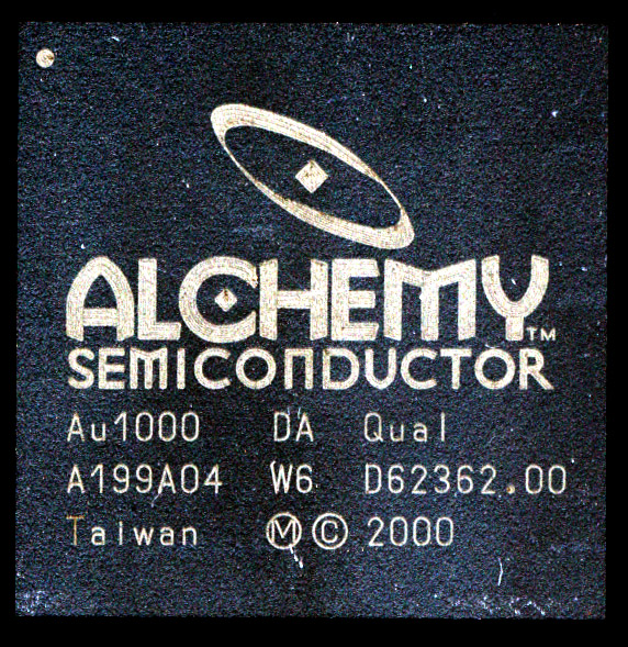
Alchemy Au1000 MIPS Processor – Qualification Sample

the thousands to vendors, system builders/integrations, and even the media outlets for review.  The hope is that nothing major wrong is found with them, and that any bugs that are found can be dealt with in software or firmware, not requiring an entire silicon fix.  Intel continues to use Q-specs for these as well, leading to some confusion with the previously mentioned ES CPU’s.  AMD usually uses part numbers beginning with ‘Z’ for QS CPU’s and like Intel, does not offer these CPU’s for sale to the general public, they are either given to vendors, or sold exclusively to them for testing.   Motorola uses XC, or XPC for these, and unlike AMD/Intel, mass produces these and sells them, often for years, before they decide that a part/design is truly fully qualified/characterized (in which case the prefixe is changed to MC. or MPC).  Texas Instruments uses the ‘TMX” prefix for their Qual. Samples. and tended to make/sell them like Motorola did with theirs, changing the prefix to TMS for fully qualified production parts.

Read More »

Posted in:
CPU of the Day

July 3rd, 2018 ~ by admin

CPU of the Day: The Intel Everest Series

Mt. Everest – Tallest on Earth

Mt. Everest is the tallest mountain here on Earth, the pinnacle of climbing challenges.  There is no going higher then Mt. Everest.  At Intel the pseudo-unofficial codename for the absolute fastest speed bin of a particular processor is…Everest.  Everest processors are the fastest an architecture will so reliably.  Sometimes these processors end up an normal products, available for consumers to purchase.  The first good example of this is the Core 2 Extreme QX9775 Yorkfield core (Core Architecture).  They were a quad-core processor running at 3.2GHz, fast but not mind blazingly so.  The Xeon equivalent was the X5492 (Harpertown) 4-core at 3.4GHz.

Xeon X5698 – Westmere – 4.4GHz – Mid 2010

The next well know Everest was a chip based on the Westmere (shrink of Nehalem) architecture.  The Westmere Everest became known as the Xeon X5698, and was available for OEMs only, in fact it was a special order processor made with one particular type of client in mind. These were to be used for High Frequency Stock traders, and other such high speed transactional processing, where the ability to complete trades as fast, and reliability as possible is the entire nature of the business.  This means that single thread performance is far more important then having multiple core, and as such, the X5698 uses a 6-core die with only 2 cores active, but retaining access to the entire 12MB of L3 cache.  Clock speed was fixed at 4.4GHz, the cores did not reduce frequency as processing demands changed, as this would introduce uncertainty in how fast it would complete a given task. Doing task ‘X’ should take a predictable amount of time and not depend on what speed the processor chose to run at.  The next fastest Westmere processor was the X5690, which was a 6-core (all cores enabled) running at 3.46GHz (the same chip essentially as the Core i7 990X).  The X5698 was nearly 1GHz faster.  The X5690 cost around $1800, where as the X5698 cost around $20,000 EACH (based on costs OEMs charged to add a 2nd one so they may have marked it up some).  The impressive thing is that these chips would go faster.  Intel sampled 4.66GHz versions and Supermicro built systems using X5698’s overclocked to 4.8GHz.  All this back in 2011.

4.4GHz Jaketown (Sandy Bridge) Everest Sample 2010-2011

Intel’s next architecture was known as Sandy Bridge.  Sandy Bridge topped at at 3.5GHz (6-cores) for the Core i7 Extreme 3970X and 3.6GHz for the 4-core i7-3820 and similar Xeon E5-1620.  Intel demo’d an air cooled Sandy Bridge running on stage for a presentation at 4.9GHz, so the core certainly had some room to spare.  There is no documentation (that I could find) that Intel actually released anything faster then 3.6GHz, at least that I could find, but evidence suggests that they at least were thinking about it.  The picture is a Sandy Bridge Xeon in LGA2011 marked JKT EVEREST SS 4.4GHZ INTERNAL USE ONLY. JKT is short for Jaketown, Intel’s codename for the 32nm Xeon E5-2600 series.  That gives a very good idea what this processor was to be.  SS is likely to be a Single Socket (as often at those speeds getting dual systems working can be tricky).  Sandy was certainly capable of hitting 4.4GHz, with 4-core, and even air cooling, so perhaps these were samples for a limited OEM run, much like the previous Westmere X5698 processors.

Read More »

June 26th, 2018 ~ by admin

Image Gallery Thumbnails working again..

Good News! The issue with the Thumbnails not working in the galleries here  has been resolved,   They aren’t super fast loading, but they do work.  This means I can start uploading a few thousand new ones.

Posted in:
Museum News

June 10th, 2018 ~ by admin

The Collector’s Guide to Vintage Intel Microchips

The CPU Shack Museum is proud to announce the availability of The Collector’s guide to Vintage Intel Microchips, written by George Phillips Jr. This e-book (PDF) contains over 1300 pages, and 900 photographs of Intel Microchips from the 1960’s and 70’s along with their functions, package variations, rarity, and valuations.  Everything from the 3101 Static RAM to the i4004 4-bit processor. The author, George Phillips, has moved this book into public domain.  Originally published back in 2007 it is still a very useful resource.  Being 10 years old, some of the values are inaccurate and there has been a few more Intel chip types from the 1970’s found since then, as well as some different package/marking variations.  However the Guide is really an important resource for any collection that includes Intel IC’s from the 1970’s.

I have been collecting information for an update to it for some time, so if you have any Intel chips/variations not in this guide, feel free to let me know.

You can download The Collector’s Guide to Vintage Intel Microchips here (pdf 22.9MB)

Posted in:
Products, Research

May 27th, 2018 ~ by admin

Mainframes and Supercomputers, From the Beginning Till Today.

This article is provided by guest author max1024, hailing from Belarus.  I have provided some minor edits/tweaks in the translation from Belarusian to English.

Mainframes and Supercomputers, From the Beginning Till Today.

Introduction

We all have computers that we like to use, but there are also more productive options in the form of servers with two or even four processor sockets. And then one day I was interested, but what is even faster? And the answer to my question led me to a separate class of computers: super-computers and mainframes. How this class of computer equipment developed, as it was in the past and what it has achieved now, with what figures of performance it operated and whether it is possible to use such machines at home, I will try to explain all this in this article.

FLOPS’s

First you need to determine what the super-computer differs from the mainframe and which is faster. Supercomputers are called the fastest computers. Their main difference from mainframes is that all the computing resources of such a computer are aimed at solving one global problem in the shortest possible time. Mainframes on the contrary solve at once a lot of different tasks. Supercomputers are at the very top of any computer charts and as a result faster than mainframes.

The need for mankind to quickly solve various problems has always existed, but the impetus for the emergence of superfast machines was the arms race of well-known superpower countries and the need for nuclear calculations for the design and modeling of nuclear explosions and weapons. To create an atomic weapon, colossal computational power was required, since neither physicists nor mathematicians were able to calculate and make long-term forecasts using the colossal amounts of data by hand. For such purposes, a computer “brain” was required. Further, the military purposes smoothly passed into biological, chemical, astronomical, meteorological and others. All this made it necessary to invent not just a personal computer, but something more, so the first mainframes and supercomputers appeared.

The beginning of the production of ultrafast machines falls on the mid-1960s. An important criterion for any machine was its performance. And here on each user speaks of the well-known abbreviation “FLOPS”. Most of those who overclock or test processors for stability are likely to use the utility “LinX”, which gives the final result of performance in Gigaflops. “FLOPS” means FLoating-point Operations Per Second, is a non-system specific unit used to measure the performance of any computer and shows how many floating-point arithmetic operations per second the given computing system performs.

“LinX” is a benchmark of “Intel Linpack” with a convenient graphical environment and is designed to simplify performance checks and stability of the system using the Intel Linpack (Math Kernel Library) test. In turn, Linpack is the most popular software product for evaluating the performance of supercomputers and mainframes included in the TOP500 supercomputer ranking, which is made twice a year by specialists in the United States from the Lawrence Berkeley National Laboratory and the University of Tennessee.

When correlating the results in Giga, Mega and Terra-FLOPS, it should be remembered that the performance results of supercomputers always are based on 64-bit processing, while in everyday life the processors or graphics cards producers can indicate performance on 32-bit data, thereby the result may seem to be doubled.

The Beginning

Read More »

April 11th, 2018 ~ by admin

PowerPC Processor for TESS Planet Hunter – Updated

TESS Orbiter – Freescale (now NXP) 2010  PowerPC e500

UPDATE: I received a note from a NASA engineer that the final flight DHU was made by SEAKR Engineering rather then Space Micro.  It turns out MIT pursued 2 different DHU systems in the design of TESS.  The Space Micro IPC 7000 was referred to as the DHU and a system by SEAKR (the Athena-3) was selected as the ADHU (Alternate Data Handling Unit).  Apparently MIT wasn’t sure which would be best so essentially characterized both (and most documentation from early on shows the Space Micro system).  In the end however, the SEAKR Athena-3 Single Board computer was selected.

If all goes well, in a few days the NASA TESS (Transiting Exoplanet Survey Satellite) will be launched on a SpaceX Falcon 9 rocket to startits mission to survey a large portion of the sky for possibly Earth-like planets.  TESS’s finds will make great candidates for further study by either Hubble, or JWST (when it finally launches).  While TESS can see transiting planets (the dimming of a star as an exoplanet passes in front of it) it cannot determine much about its composition, or the composition of its atmosphere.  However, having a list of exoplanets to further check out, especially Earth-sized ones, it’s a big help.  TESS was created as part of the NASA Medium Class Explorers Program (MIDEX) which is for mission up to around $200 Million total cost to NASA (not including launch).  TESS itself cost about $75 million (developed in large part by MIT and built by Orbital-ATK on their LEOStar-2 Platform) and the launch services contract was $87 Million with the remainder taken by operations and contingency funding.

Space Micro Proton 400k with Freescale 2020 processor

That makes this one of the least expensive NASA missions, but one that has engendered much more public interest then its cost suggests.  Finding alien worlds captivates people hearts and minds.  So what is at the heart of the TESS orbiter?  Obviously the premier technology is its 4 cameras that will scan the sky, but the computer that powers these is no less interesting.

The 4 cameras are interfaced to a Data Handling Unit (DHU).  Initially the DHU was to be the Space Micro IPC-7000 computer.  The IPC-7000 consists of a TI TMS320C67xx 32-bit DSP and a pair of Xilinx Virtex-7 FPGAS.  They handle all the pre-processing of the imagery collected by the cameras, making it into a format that is easily transmitted back to earth.  The rest of the spacecraft functions (such as actually sending/storing the data and other space craft house-keeping) is handled by a Space Micro Proton 400k SBC.  The Proton 400k is based on a Freescale 2020 1GHz Dual Core PowerPC processor made on a 0.45u process..  Each PowerPC e500v2 core has a 7-stage pipeline with 32K of I-cache and 32K of D-Cache and shares a single 512K L2 Cache.  The computer also containing a pair of 192GB solid state memory boards for buffering imagery data (data is relayed to Earth only once per orbit, so it needs to store data from around 14 days).

Athena-3 SBC – Powered by a 1.067GHz Freescale P2010 Processor

The final flight version of TESS switched to an ADHU made by SEAKR Engineering.  This uses a very similar setup but a bit less powerful processor.  The heart of the ADHU is the Freescale P2010 e500 processor at 1066MHz with 1GB of DDR2 RAM and 1-4GB of Flash.  This is the single core version of the P2020 used in the initial Proton 400k.  The ADHU also includes a RCC5 triple Xilinx Virtex-5 FPGA board to handle additional camera processing functions (and anything else not handled by the P2010 processor).  Solid state storage is a Gen 3 FMC also by SEAKR, containing 3 boards with a total of 192GB of Flash.  The ADHU handled all of the science, processing the raw camera data into useful science data and handling the sending of data to the 100-125MBit/sec Ka-band transmitter.  It also supplies some star reference information used by the MAU (Master Avionics Unit) computer to provide finer attitude control of the satellite.  The MAU is the LeoStar-2 Satellites main computer, and handles all the mechanics of flying the spacecraft outside of the science work done by the ADHU.

Freescale P2020 Processor

In many ways this is a very advanced processor compared to the RAD750 processors we often see on large scale NASA missions.  The Freescale 2020/2010 is not an inherently radiation hardened design, however both Space Micro and SEAKR  implements many radiation mitigating designs in the system design to compensate for this.  It is not as robust as the RAD750 but it is a $75 million earth satellite with a target mission life of 2-years so it doesn’t need to be. The 2020 processor does give TESS tremendous processing power for a scientific satellite, allowing for a lot of pre-processing of the imagery.  This allows TESS to handle much of the grunt work, and send scientists here on Earth only the very best data, in a format that is the most useful to them.


Tags:
,

Posted in:
CPU of the Day

March 24th, 2018 ~ by admin

Making MultiCore: A Slice of Sandy

Intel Sandy Bridge-EP 8-core dies with 6 cores enabled. Note the TOP and BOTTOM markings (click image for large version)

Recently a pair of interesting Intel Engineering Samples came to The CPU Shack.  They are in a LGA2011 package and dated week 33 of 2010.  The part number is CM8062103008562 which makes them some rather early Sandy Bridge-EP samples.  The original Sandy Bridge was demo’d in 2009 and released in early 2011.  So Intel was making the next version, even before the original made it to market.  The ‘EP’ was finally released in late 2011, over a year after these samples were made.  Sandy Bridge-EP brought some enhancements to the architecture, including support for 8-core processors (doubling the original 4).  The layout was also rather different, with the cores and peripherals laid out such that a bi-direction communications ring could handle all inter-chip communication.

Sandy Bridge-EP 8-core die layout. Note the ring around the inside that provides communications between the peripherals on the top and bottom, and the 8-cores. (image originally from pc.watch.impress.co.jp)

Sandy Bridge EP supports 2, 4, 6 and 8 cores but Intel only produced two die versions, one with 4 cores, and one with 8 cores.  A die with 4 cores could be made to work as a dual core or quad, and an 8-core die could conceivably be used to handle any of the core counts.  This greatly simplifies manufacturing.  The less physical versions of a wafer you are making, the better optimized the process can be made.  If a bug or errata is found only 2 mask-sets need updated, rather then one for every core count/cache combination.  This however presents an interesting question..What happens when you disable cores?

That is the purpose of the above samples, testing the effects of disabling a pair of cores on an 8-core die.  Both of the samples are a 6-core processor, but with 2 different cores disabled in each.  One has the ‘TOP’ six cores active, and the other the ‘BOTTOM’ six cores are active.  This may seem redundant but here the physical position of the cores really matters.  With 2 cores disabled this changes the timing in the ring bus around the die, and this may effect performance, so had to be tested.  Timing may have been changed slightly to account for the differences, and it may have been found that disabling 2 on the bottom resulted in different timings then disabling the 2 on the top.

Ideally Intel wants to have the ability to disable ANY combination of cores/cache on the die.  If a core or cache segment is defective, it should not result in the entire die being wasted, so a lot of testing was done to determine how to make the design as adaptable as possible.  Its rare we get to see a part from this testng, but we all get to enjoy its results.

March 21st, 2018 ~ by admin

Intel’s Chipped Chips

Early Intel 8080A processor (no date code) chipped and used in a Uni kit

Typically when collecting something, be it coins, cars or CPU’s having the most pristine unblemished example is highly desirable.  However, sometimes, the best example is one that isn’t perfect, in coin collecting it may be a rare double struck coin, or some other flaw that actually makes the coin more valuable.

In the 1970’s Intel put together many development kits for it’s processors.  These were to help engineers, companies, and even students learn how to use Intel’s products. Intel made several kits specifically for University use, including one based around the MCS-80 processor and another around the MCS-48 microcomputer.  The 8080 University kit came with an 8080 processor, and a variety of support chips, including RAM, EPROMs (usually 1702s), clock drivers, bus drivers etc.  They were often a mix of packages, including plastic, and ceramic, with many chips being marked ‘CS‘ which is Intel’s designation for a Customer Sample.

Military MC8080A CS from a Uni kit. Multiple chipped corners. Such damage often was a result of improper packing in an IC shipping tube.

The price of the kits was kept low, the purpose was to get people use to using Intel products, not to make money.  Due to this, Intel tried to build the kits in the most efficient way possible.  Almost every 8080 University kit included a working, but cosmetically damaged C8080A processor.  These were typically the white/gold ceramic variety with a chipped corner.   It was very common to see a MC8080A or MC8080A/B military spec processor in a University kit, the processor would function fine, but had  some damage, enough that it could not be sold as a mil-spec processor (which has requirements for screening out such damage). The damaged chip would simply be tested, stamped ‘CS‘ and stuck in a kit, ths saving Intel money and keeping a working processor from being wasted.   The same thing happened with the MCS-48 University kits, these included chips such as the D8035 or C8748 MCU, and again, often shipped with damaged chips.

It turns out that the most correct, authentic chip, in a University Kit, was the cosmetically challenged, and in a way, this makes them more uncommon and more interesting.  Its due to their damage that they were selected for the special use in a University kit.  The irony is that many times it was the highest end military screened chips, that ended up getting used in one of the lowest end products.

March 15th, 2018 ~ by admin

CPU of the Day: Intel Jayhawk – The Bird that Never Was

Intel Jayhawk Thermal Sample – 80548KZ000000 QBGC TV ES – Made in April 2004 Just 3 weeks before it was canceled

Perhaps fittingly the Jayhawk is not a bird, but rather a term used for guerilla fighters in Kansas during the American Civil War.   It is also the name of a small town in California 150 miles Northeast of Intel’s headquarters in Santa Clara.  It was also the chosen code name for a Processor Intel was working on back in 2003.  In 2003 Intel was working on the Pentium 4 Prescott processor, to be released in 2004 and its Xeon sibling, the Nocona (and related Irwindale),  The Prescott was a 31 stage design made on a 90nm process.  There was hopes it would hit 4+ GHz but in production it never did, though overclockers, with the help of LN2 cooling were able to achieve around 8GHz.  Increasing the length of the pipeline helps allow higher clock speeds, the Northwood core had a 20-stage pipeline so the Prescott was a rather big change.  There is a cost of lengthening the pipe, processors don’t always execute instructions in order, often guessing what will come next to speed up execution.  This is called speculative execution, processors also guess what data is to be needed next, and stick it in cache.  If either of these ‘guesses’ is wrong, the processor needs to flush the pipeline and start over, at a comparatively massive hit in performance.  This is what performance doesn’t always scale very linearly with clock speed.

Intel figured that this wouldn’t be an issue and so the Prescotts successor was to have a 40-50 stage pipeline.   THe hopes were for 5GHz at 90nm and 10GHz at 65nm. The desktop version was known as Tejas, and the server version, Jayhawk.  Initially these were to be made on the 90nm process, same as Prescott, before being transitioned to a 65nm process.  It increased the L1 cache to 24k (some sources say 32k) from the Prescotts 16k.  The Instruction trace cache was still 16k micro-ops, though this could have been increased.  L2 cache would have been 1MB at introduction and 2MB once the processor moved to a 65nm process.  Eight new instructions were to be added called ‘Tejas New Instructions’ or TNI, these later would become part of the SSSE3 instructions released with the Core 2 processor.  It also would bring ‘Azalia’ Intel’s High definition audio codec, DDR2 support, a 1066MHz bus, and PCI-Express support.  It turns out there was a problem….

Read More »

January 28th, 2018 ~ by admin

CPU of the Day: Tandem CLX 800 – It Takes 2 To Tango

TANDEM CLX 800 Processor – VLSI CMOS 1u process – 16MHz.

Tandem Computers was established way back in 1974, and was one of the first (if not the first) dedicated fault-tolerant computing companies.  They designed completely custom computers designed for use in high reliability transaction processing environments.  These were used for support of stock exchanges, banks, ATM networks, telephone/communications interchanges, and other areas where a computer failure would result in significant, costly, disruptions to business services.  Tandem was started by James Treybig, formally of HP, and a team he lured away from HP’s 3000 computer line.

Tandem computers are designed to do two things well, fail-over quickly when a failed part is detected.  This means that if a faulty processor or memory element is found, it can be automatically disabled, and processing continues, uninterrupted, on the rest of the system.  The other design element that Tandem perfected was allowing the computer to find and isolate intermittent problems.  If a processor or storage element ceases to work, that is relatively easy to figure out, but if a processor is glitchy, causing errors only occasionally, that can be much harder to find and can result in serious problems for the user.  This is known as ‘Fast Fail’ and today is a pretty standard concept, find the error, catch it, and prevent erroneous data from ever making it back into the database.  Tandem computers were designed from the ground up to be fault tolerant, disks were mirrors, power supplies, busses,

Tandem CLX 600 PCB (click for larger)

processors,all were redundant, but unlike some other systems, components were not kept as ‘hot spares’ sitting idle until something failed.  This kept hardware from being ‘wasted.’ Under normal operation if it was in the system, it was contributing to system performance.  A failed component then would reduce system performance until it was replaced/fixed, but a customer would not be paying for hardware that served them no purpose unless something broke.

To support these goals Tandem designed their own processors and instruction set architecture know as TNS (Tandem NonStop).  The first processors were a 16-bit design call the T/16 (later branded NonStop I) made out of TTL and SRAM chips spanning 2 PCBs.  Performance was around 0.7MIPS in 1976.  They were a stack based design similar to the HP3000 with added registers as well.  T/16 systems supported 2-16 processors. NonStop II, released in 1981, was similar, but supported the occasional 32-bit addressing, increasing accessible memory form 1 to 2MB per CPU and performance to 0.8MIPS.

The 1983 introduction of TXP saw a great performance improvement, up to 2.0 MIPS, but kept the same form factor.  The processor was implemented in TTL, with the addition of many PALs and added much better support for 32-bit addressing.  In 1986 the NonStop VLX was released, which moved to an ECL based processor.  This was a full 32-bit design, running at 12MHz (3MIPS) but still using discrete components and a new bus system as well.  This was to be the high end of the NonStop line, it was fast reliable, and rather large.  The desire for a more economical system to fit the needs of smaller customers led to a first for Tandem…

Read More »

Posted in:
CPU of the Day