June 27th, 2021 ~ by admin

Navy Hydrophone Noise Canceller: Weitek 3332 Floating Point Based DSP

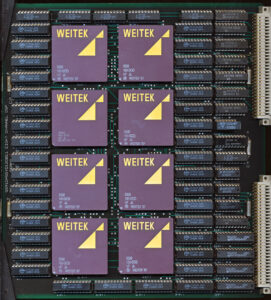
Navy 55910 ASSY 0120811 Eight Channel DSP – Serial #1

I got these boards some time ago, hoping to be able to figure out more about them but alas, information is very sparse, but they are such good looing boards, with impressive technology for the day, I had to post them

These boards came out of a US Navy system labeled “Hydrophone Noise Canceller”  which seemed to be part of SONAR test system at a University.  These date from the late 1980’s to the early 1990’s. The system was comprised of 16 boards, 12 8 Channel DSP board, a control board, and 3 Ethernet Boards,  Each of these boards is a very heavy 4 layer PCB, with pretty much everything socketed.

The DSP Boards are based on the Weitek 3332 FPU. These are full 32-bit Floating point datapaths (MULT/DIV/ADD/SUB + Registers) and made on a CMOS process.  They operate on a 100ns (10MHz) clock.  THese are the higher end version of the 3132, they have a full 3 busses versus the single bus of the 3132.  These 3 busses add a lot to the pincount (168 vs 144) and thus cost but make designing a system more flexible, no bus sharing to worry about.  The 3332 was designed specifically to support high speed DSP and graphics processing.  It performed the ‘core’ of a DSP, allowing the user to build around it and make essentially a custom DSP for their application (unlike the purpose built TI TMS320 series of DSPs also available at them time) On the board they are backed by 4 Cypress CY7C128 2K SRAM per processor (8K total).  There is no clock crystal on the board itself, which is typical of a system like this.  To ensure everything stays in synch, the clock would be provided by the control board and distributed to each of the boards on the bus.

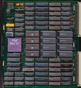
Navy 55910 ASSY 0125321 Controller A80386DX-25 (20MHz) Serial #2

The Control Board runs an Intel A80386DX processor.  On this particular board its a 25MHz chip, but note the crystal next to it is an 80MHz crystal.  A 386 internally divides the clock by 2, so the 80MHz clock is most like divided by 2 externally resulting in a 40MHz input to the 80386, and a 20MHz CPU clock.  I had another controller board with a 20MHz 80386 so they probably just used what ever they had available.  This is Serial # 2 afterall.  The 386 is supported by 4 27C256 EPROMs and 8 32K (CY7C198) SRAM chips, giving it 256K of SRAM.  In addition is 12 8k (CY7C185) 8K SRAM chips each with there own Pipeline Register.

A typical 386 system would have several MB of RAM, but this system is set up for real time data processing, as a DSP system, so the only data that needs to be in RAM is the control program itself, so 256K of system RAM is a great plenty.  Additional RAM is likely used solely for buffering data from the Hydrophones.

It would be interesting to know what this board was used for in more detail, but even if that never happens its an interesting board for its time.  Clearly a vast amount of effort went into designing and building the system.


Tags:
,

Posted in:
Boards and Systems
September 30th, 2018 ~ by admin

Peavey and the Motorola DSP56000

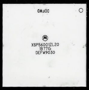
Motorola XSP56001ZL20 – 20.5MHz 1990

In 1985 Motorola was looking to create a DSP (Digital Signal Processor) line of processors to go with their very popular 68000 series of general purpose processors.  DSP’s are similar to a normal processor but, as their name implies, are designed to work on signals, versus data stored in memory.  Typical signal data is audio, video, RF (such as RADAR information) and anything else that comes in via an ADC.  These signals are processed via algorithm such as FFTs (Fast Fourier Transforms) to manipulate, change or analyse them.  In audio, this can be used for cleaning up an audio stream, adding effects to it, or even generating audio.

In the 1980’s the main single chip DSP competitors was the still in use TI TMS320 series. the ATT/WE DSP16 series, and some DSP’s from OKI/NEC.  When Motorola began work on what would become the DSP56000 they asked one of their long time customers, Peavey, what they would like to see in a DSP. Peavey is an audio equipment manufacturer, making such things as guitar amps and keyboards, so would have a good idea of what would be useful in a DSP designed for audio signals.

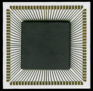
These were packaged in a ‘SLAM’ package. The contacts/traces were easily damaged by leaking batteries.

The DSP5600 is a 24-bit processor made on a 1.5u HCMOS process with around 150,000 transistors.  24-bits were selected as that was ideal for audio sampling at the time (and most ADS/DACs at the time max’d out at 20-bits of resolution anyways.  These DSP’s had a 3-stage pipeline and ran at 20.5MHz, 27MHz and 33MHz.  This provided around 10.25 MIPS of performance (at 20.5MHz).  They were a fixed point (no floating point support in hardware) design, which was adequate at the time.  A total of 62-instructions were provided.

The DSP56001 is identical to the DSP56000 except that it has 512×24-bits of on-chip program
RAM instead of 3.75K of program ROM and a 32×24-bit bootstrap ROM for loading the program RAM.  This is the version that became most popular.  Peavey used the 560001 (3 of them actually) to power the DPM3 SE keyboard back in 1990.  Recently J. Acorn, from Crasno Electronics in Canada sent The CPU Shack Museum an e-mail inquiring if I had a few of these now obsolete 56001 DSPs spare, to rebuild some dead Peavey keyboards.   As a Museum, I not only like to collect and present vintage IC’s but also regularly help people with project such as this, and have thousands of CPU’s sitting around that have been acquired through the years (really its a bit crazy how much I have collected lol).  Mr. Acorn needed 2 of these DSPs to replace ones destroyed by a leaking battery in a keyboard, and two is exactly what I had spare.  I dug them out, packaged them, and off to Canada they went.  The result?  A restored and working Peavey keyboard.  You can read about the restoration process on Crasno’s site.

The 56000 series continued to be made by Motorola (and then Freescale) up until 2012 when it was announced it would be discontinued as a standalone product.  The 56000 series cores though live on, inside of other Freescale (now NXP) products.


Posted in:
CPU of the Day

December 19th, 2017 ~ by admin

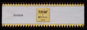
Chip of the Day: TRW MPY-16AJ – Making Multiplication Manageable

TRW MPY16AJ – 1978

In Primary School students are tasked with memorizing their multiplication tables.  Taking the time to manually calculate 6×5 is much slower than simply committing the result to memory.  This allows more complex math to be processed quicker as the students skills develop.  Typically this is limited to numbers up to 12×12, resulting in 144 results to ‘store.’  In computing the same can be done.  A ROM can be used as a lookup table for multiplication.  The problem is it does not scale well.  Handling 4×4-bit multiplication requires a 256×8 ROM (2m+n addresses and m+n outputs). This could be handled by a many ROMs available in the 1970’s.  Anything more than 4-bits though was simply not possible.  This gave rise to the need for multipliers to calculate the result.

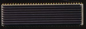
TRW MPY16AJ – Large Heatsink affixed to package to dissipate its 5W

This was a problem TRW set out to rectify in 1976.  TRW LSI Products was formed in the 1960’s to commercialize the transistor products that had been developed by Pacific Semiconductors, a division of TRW.  It was James Buie who invented the TTL logic gate in 1961 while working for TRW.  TTL went on to become the logic standard throughout the 1970’s and 80’s.   TRW was involved in aerospace, helping design planes, satellites, and missiles, fields that required processing of signals data, what became known as Digital Signal Processing (DSP).  In the 1980’s processors were designed to handle this, such as the TI TMS320 series, but in the 1970’s it had to be done with discrete components.  DSP systems had several needed blocks, Fast ADCs, ALUs, and multipliers.  TRW invented fast ADCs to handle the inputs, and ALUs were available such as AMDs Am2901 or even the TTL series 74181s.  Multipliers however were not widely available, especially for large bit-widths.

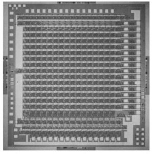
MPY-16 die

TRW’s first multiplier was a custom device to work with their own avionics processing system.  It was made on a Bipolar process, and multiplexed the entire product, using around 40 pins total (the entire product was multiplexed with the operands).  It could handle a multiply in 330ns worst case.  Interestingly yields of the device were considered ‘excellent’ at 3 working devices per wafer (out of 19 per wafer (most likely a 2″ wafer)).  Today, yields like that would be completely unacceptable.

TRW designed the MPY-16AJ as a brute-force 16×16 multiplier.  It was designed on a Bipolar process with around 3600 gates.  It implements a series of AND gates and CARRY-SAVE-ADDERS to implement the multiplication.  There are faster methods, but they come at the cost of complexity and power draw.  As designed the the MPY-16AJ dissipates 5 Watts while handling a signed (2’s complement) multiplication in a worse case 230ns).  They MPY16 was packaged in a large 64-pin package to limit the # of pins that had to be multiplexed.  The lower 16-bits of the product are multiplexed with one of the operands.  This is acceptable as in many applications the upper 16-bits of the product are sufficient accuracy.  The 64-pin package allowed for not less multiplexing, but also a much larger surface for heat dissipation.  A heatsink was also affixed to the package as well.

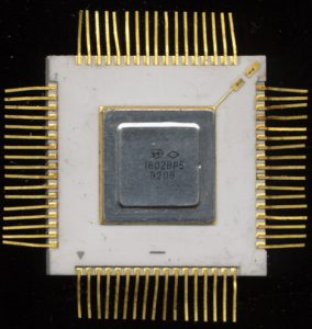
Micron (Russia) 1802VR5 – MPY16HJ Clone made in 1992

Later versions of the MPY-16 added support for unsigned multiplication as well (the MPY16H) and became the standard for 16-bit multipliers.  Compatible multipliers were made by Analog Devices (ADSP1016, 40-50ns at 150mW) and LOGIC LMU16/216) in CMOS, by Weitek (WTL1516/A/B, 50-100ns at 0.9-1.8W) in NMOS, by Synertek (SY66016 100ns at 1.5W) in HMOS, by AMD (Am29516 38ns at 4W) in ECL, as well as many others.  These were implemented internally with different processes, and different multiplier algorithms but externally they all mimicked the standard TRW MPY16J and served as the basis of many signal processing and high end math computers.  As a testament to their usefulness, the MPY16 was also copied by the USSR as the 1802VR5.  The TRW MPY16 was last made in the mid-1980’s but its clones continued to be made into the 1990’s.  Today its functions can be handled by any DSP, CPU or even coded into a FPGA, but for a time, the MPY16 multiplied the efficiency of many processing systems.

Tags:
, ,

Posted in:
CPU of the Day

March 17th, 2011 ~ by admin

Chips of the day: TI TMS320E The tale of the two dies

Its fairly common for a manufacturer to make several devices out of a single actual die.  Just disable part of the die, whether because its faulty, or not needed, or simply do not connect the pins to that feature.  Intel did this a lot with the Celeron, and PIII line, disable some L2 cache on a PIII and you get a Celeron.  Today it is done with multi-core processors.

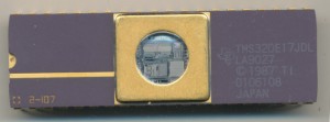
TI TMS320E17JDL

Using a common wafer for several products saves a large amount of money, no need for a second mask set, and testing systems.  Here we have a Texas Instruments TMS320E17JDL.  The TMS320 is the industry standard in DSPs (Digital Signal Processors). The E17  from 1990 runs at 20.5MHz has a 4K EPROM, 256 bytes of RAM, and a pair of serial ports.  You can see the large sections of the die devoted to the ROM, RAM, and MAC (Multiply and Accumulate).

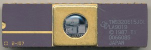
TI TMS320E15JDL

This is the TI TMS320E15JDL.  It is the same basic DSP core as the E17, it includes the same 4K EPROM, the same 256 bytes of RAM and the same MAC unit.  It has some I/O ports tasked with doing different things, but thats a relatively minor difference.  The big difference is the E15 lacks the 2 serial ports of the E17.  You can see on the die where that hardware does not exist, its a large black spot, void of any circuitry.  A very interesting and unusual occurrence.

TI either used a completely different mask for the E15, or they simply chose to not expose that small part of the mask.

Tags:
,

Posted in:
CPU of the Day

November 16th, 2010 ~ by admin

The History of the SMS300 and Signetics 8X300 Processors

On November 20th, 1969 a small company was formed in Mountain View, CA called Scientific Micro Systems Inc (SMS). They would join the dozens of post-Fairchild semiconductor startups in Silicon Valley.  Many of these we remember and know well, Intel, AMD, Zilog, MOS all are familiar and have designed processors that left a story, if not a legacy, in history. SMS has became a forgotten player in the roaring 70’s but they did introduce a few important things to the market. First 4096-bit bipolar Schottky ROM? SMS. First 256-bit bipolar Schottky RAM? Again SMS.

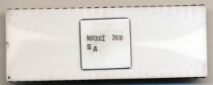
Signetics N8X300I – Early 1978

In January 1975 SMS announced prototypes of their own 8-bit microcontroller.  The SMS300 was a non-traditional design.  It focused on manipulation of signals.  It had 16-bit instructions, but operated on data 8 bits at a time.  It had very limited ways of accessing external memory (and no real way to access data memory).  It was designed as perhaps the first DSP.  It was fabricated in bipolar Schottky transistor technology.  This allowed it to be incredibly fast (albeit very power hungry) for its time.  Initial clock speeds were 6.66MHz and quickly ramped to 8MHz in 1976.  The SMS300 was initially not available for sale as a single chip.  It was sold as a single board computer called the SMS330 (as well as the SMS331 and SMS332) which contained everything needed to run the SMS300.  This was packaged like a oversized 64pin DIP (similar to how some of the BASIC Stamp microntrollers are today). These systems started at $370 and topped out at $1460.  In August of 1975 SMS ‘unbundled’ the SMS300 and began selling it (and its support chips) separately to those who wanted them.

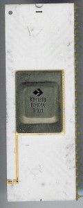
Soviet Electronika KM1818VM01A 8X300 Clone

Soviet Electronika KM1818VM01A 8X300 Clone

SMS did not make the SMS300 themselves, they contracted another Silicon Valley company to fabricate them.  Signetics, founded in 1961 by ex-Fairchild workers, was the first company founded to solely manufacture ICs rather then discrete transistors.  In 1975 Signetics was purchased by Philips but continued to operate under the Signetics trademark until 1993. Signetics made all of the SMS300 devices for SMS, and in 1976 Signetics became a second-source, and could sell the SMS300 under the Signetics brand.  By 1978 Signetics had purchased the rights to the SMS300 and renamed it the 8X300.  1977 or 1978 is generally when people think the 8X300 was develped. This is, unfortunately, due to forgotten history as by the time Signetcs bought the design, it had been on the market and in use for over 2 years.  Signetics continued to make the 8X300 into the early 1990s where it found wide use in disk controllers, telecommunications and other DSP like environments.  The N8X300 was also second sourced by AMD though I have yet to see one.  The 8X300 was also *second sourced* by the Soviets in the 80’s and early 90’s by the Electronika state electronics company in what is now Voronezh, Russia.  These of course were not licensed copies but they are however, still of interest.

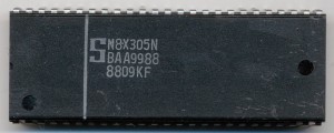
Signetics N8X305N Early 1988

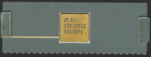
In around 1982 Signetics released the N8X305, the successor to the 8X300.  It was functionally compatible but increased the general purpose registers to 13 from 8 among some other instruction improvements that greatly improved upon the data handling deficiencies of the 8X300. Processor speed was also boosted to 10MHz. (200ns instruction time vs 250ns for the 8X300) The N8X305 also used the same pin-out as the 8X300 and the same 50pin DIP package (as well as adding a 68pin PLCC).  AMD second-sourced the 305 as the AM29X305.  The N8X305 continued to be made into the 1990s and saw use in many military applications as well.  Because of this Signetics/Philips could not simply terminate production.  They sold production rights to Lansdale Semiconductor Inc., who still offers the N8X305 to this day.

Signetics N8X401I – 1988

In 1986 Signetics again revised the design and released the N8X401.  This processor now had a full 32 instruction (including a RETURN instruction allowing the use of subroutines) The N8X401 also added an 8-bit data bus making data handling somewhat simpler but also increasing the package size to a 64 pin DIP.  Internal usable registers was increased to 16 and the instruction width was increased to 20-bits. Clock speed remained at 10MHz but it was now fabricated in ECL (Emitter Coupled Logic).  This among other improvements, helped to result in a 35% speed boost over the N8X305.

AMD AM29X305DC – N8X305 Second Source – 1985

The N8X401 was not a great success, primarily because of the competition at the time.  By 1986 8-bits, even for a DSP, was rapidly becoming out of date, especially with such purpose built DSPs such as the Motorola DSP56000 and the industry standard setting TI TMS320 series.

Thus is the story of one of the most odd processors to come out of the chip boom of the 1970’s (EA 9002, MMI 6701, AMI S2000 et al).  There are several other forgotten processors of that era which are also deserving of some remembrance.  In time we’ll try to document their history here at the CPU Shack as well.

Posted in:
Research