January 28th, 2018 ~ by admin

CPU of the Day: Tandem CLX 800 – It Takes 2 To Tango

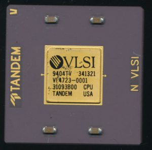
TANDEM CLX 800 Processor – VLSI CMOS 1u process – 16MHz.

Tandem Computers was established way back in 1974, and was one of the first (if not the first) dedicated fault-tolerant computing companies.  They designed completely custom computers designed for use in high reliability transaction processing environments.  These were used for support of stock exchanges, banks, ATM networks, telephone/communications interchanges, and other areas where a computer failure would result in significant, costly, disruptions to business services.  Tandem was started by James Treybig, formally of HP, and a team he lured away from HP’s 3000 computer line.

Tandem computers are designed to do two things well, fail-over quickly when a failed part is detected.  This means that if a faulty processor or memory element is found, it can be automatically disabled, and processing continues, uninterrupted, on the rest of the system.  The other design element that Tandem perfected was allowing the computer to find and isolate intermittent problems.  If a processor or storage element ceases to work, that is relatively easy to figure out, but if a processor is glitchy, causing errors only occasionally, that can be much harder to find and can result in serious problems for the user.  This is known as ‘Fast Fail’ and today is a pretty standard concept, find the error, catch it, and prevent erroneous data from ever making it back into the database.  Tandem computers were designed from the ground up to be fault tolerant, disks were mirrors, power supplies, busses,

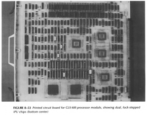
Tandem CLX 600 PCB (click for larger)

processors,all were redundant, but unlike some other systems, components were not kept as ‘hot spares’ sitting idle until something failed.  This kept hardware from being ‘wasted.’ Under normal operation if it was in the system, it was contributing to system performance.  A failed component then would reduce system performance until it was replaced/fixed, but a customer would not be paying for hardware that served them no purpose unless something broke.

To support these goals Tandem designed their own processors and instruction set architecture know as TNS (Tandem NonStop).  The first processors were a 16-bit design call the T/16 (later branded NonStop I) made out of TTL and SRAM chips spanning 2 PCBs.  Performance was around 0.7MIPS in 1976.  They were a stack based design similar to the HP3000 with added registers as well.  T/16 systems supported 2-16 processors. NonStop II, released in 1981, was similar, but supported the occasional 32-bit addressing, increasing accessible memory form 1 to 2MB per CPU and performance to 0.8MIPS.

The 1983 introduction of TXP saw a great performance improvement, up to 2.0 MIPS, but kept the same form factor.  The processor was implemented in TTL, with the addition of many PALs and added much better support for 32-bit addressing.  In 1986 the NonStop VLX was released, which moved to an ECL based processor.  This was a full 32-bit design, running at 12MHz (3MIPS) but still using discrete components and a new bus system as well.  This was to be the high end of the NonStop line, it was fast reliable, and rather large.  The desire for a more economical system to fit the needs of smaller customers led to a first for Tandem…

Read More »

Posted in:
CPU of the Day

June 5th, 2017 ~ by admin

SiFive FE310: Setting The RISC Free

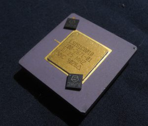
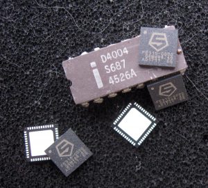
SiFive FE310 RISC-V Processor. Early LSI SPARC Processor for size comparison. Both are based on U.C. Berkeley RISC designs.

The idea of RISC (Reduced Instruction Set Computer) processors began in education, specifically University of California, Berkeley in the early 1980’s, and it was out universities that some of the most famous RISC designs came.  MIPS, still in use today, started life as a project at Stanford University, and SPARC, made famous by Sun, and now made by Oracle and Fujitsu, started life as a Berkeley University project.  Universities have continued to work with RISC architectures, for research and teaching.  The simplicity of RISC makes them an ideal educational tool for learning how computers/processors function at their basic levels.

By the late 1980’s RISC had begun to become a commercial revolution, with nearly every player having their own RISC design.  AMD (29k), Intel (i960), HP (PA-RISC), Weitek (XL8000), MIPS, SPARC, ARM, Hitachi (SH-RISC), IBM (POWER), and others offered their take on the RISC design.  Most were proprietary, while a few were licenseable, none were open architectures for anyone to use.

Unfortunately, outside of the university, RISC processors are not as simple.  The architectures, and their use may be, but licensing them for the design is not.  It can often take more time and effort to license a modern RISC processor then it does to actually implement it.  The costs to use these architectures,both in time and money often prohibit their very use.

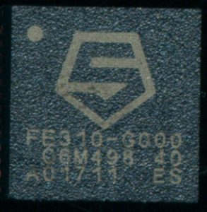
SiFive FE310 – Sample Donated by SiFive. Full 32-bit RISC on a 7.2mm2 die in a ~36mm2 package

It is out of this that SiFive began.  SiFive was founded by the creators of the first commercially successful open RISC architecture, known as RISC-V.  RISC-V was developed at Berkeley, fittingly, in 2010 and was designed to be a truly useful, general purpose RISC processor, easy to design with, easy to code for, and with enough features to be commercially useful, not limited to the classroom.  It is called the RISC-V because it is the fifth RISC design developed at Berkeley, RISC I and RISC II being designed in 1981, followed by SOAR (Smalltalk On A RISC) in 1984 and SPUR (Symbolic Processing Using RISC) in 1988.  RISC-V has already proved to be a success, it is licensed freely, and in a way (BSD license) that allows products that use it to be either open, or proprietary.  One of the more well known users is Nvidia, which announced they are replacing their own proprietary FALCON processors (used in their GPUs and Tegra processors) with RISC-V.  Samsung, Qualcomm, and others are already using RISC-V.  These cores are often so deeply embedded that their existence goes without mention, but they are there, working in the background to make whatever tech needs to work, work.

The RISC-V architecture supports 122 instructions, 98 of which are common to almost all prior RISC designs and 18 common to a few.  Six completely new instructions were added to handle unique attributes of the architecture (using a 64-bit Performance Register in a 32-bit arch.) and to support a more powerful sign-injection instruction (which can be used for absolute value, among other things). It uses 31 32-bit registers (Register 0 is reserved for holding the constant ‘0’) with optional support for 32 floating point registers.  True to the RISC design, it is a pure Load/Store processor, the only accesses to memory are via the Load/Store instructions.

Intel 4004 with 5 SiFive RISC Processors. The 4004 was meant for a calculator. The FE310 is meant for whatever your mind may dream up.

SiFive is unique among RISC IP companies.  They not only license IP but also sell processors and dev boards.  The FE310 (Freedom Everywhere 310) is a 320MHz RISC-V architecture with 16K of I-cache and 16K of scratchpad RAM fabbed by TSMC on a 180nm process. Even on this process, which is now a commodity process, the FE310’s efficient design results in a die size of only 2.65mm x 2.72mm.  On a standard 200mm wafer , this results in 3500 die per wafer, greatly helping lower the cost.  Its an impressive chip, and one that is completely open source.  What is more impressive is licensing SiFive cores, it is a simple and straightforward process.  The core (32 bit E31 or 64-bit E51) can be configured on SiFive’s site, with pricing shown as you go.  The license is a simple 7 page document that can be signed and submitted online.  Pricing starts at $275,000 and is a one time fee, there are no continuing royalty payments.  The entire process can be completed in a week or less.

In comparison, ARM, the biggest licensor of RISC processors, does not publish pricing, charges 1-2% royalties on every chip made, and has a license process that can take over a year.  The base fees start at around $1 million and go into the 10’s of millions, depending on how you want to use the IP, where it will be, and for how long.  For many small companies and users this is simply not feasible, and it is these smaller users that SiFive wishes to work with.  Licensing a processor for the next great tech, should not be the hurdle that it has become.  Many great ideas never make it to fruition due to these roadblocks.  We look forward to finding SiFive processors and cores in all sorts of products in the future.

Thanks to SiFive for their generous donation of several FE310 processors to the CPU Shack Museum.

Tags:
, , , ,

Posted in:
CPU of the Day

February 27th, 2014 ~ by admin

The Unlikely Tale of How ARM Came to Rule the World

Bloomberg Business Week recently published an interesting article on ARM’s rise to power in the processing world.  There first major design ‘win’ was a failed product known as the Apple Newton, yet they would go on to become a powerhouse that is no challenging Intel.

In ARM’s formative years, the 1990’s, the most popular RISC processor was the MIPS architecture, which powered high end computers by SGI, while Intel made super computers (the Paragon) based on another RISC design, the i860.  Now, nearly 2 decades later, after Intel abandoned their foray into the ARM architecture (StrongARM and X-Scale) RISC is again challenging Intel in the server market, this time, led by ARM.

MIPS, now owned by Imagination, is again turning out new IP cores to compete with ARM, and other embedded cores.  Their Warrior class processors are already providing 64-bit embedded processing power, though with a lot less press that the likes of Apple’s A7.

Tags:
,

Posted in:
Processor News

November 17th, 2013 ~ by admin

Itanium is Dead – And other Processor News

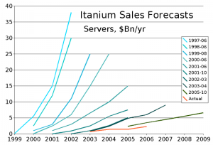
Itanium Sales Forecasts vs Reality

Itanium Sales Forecasts vs Reality

‘Itanium is dead’ is a phrase that has been used for over a decade, in fact many claimed that the Itanium experiment was dead before it even launched in 2001.  The last hold-out of the Itanium architecture was HP, likely because the Itanium had a lot in common with its own PA-RISC.  However HP has announced that they will be transitioning their NonStop sever series to x86, presumably the new 15-core Xeons Intel is developing.  Itanium was launched with goal of storming the server market, billed as the next greatest thing, it failed to make the inroads expected, largely due to the 2 decades of x86 code it didnt support, and poor initial compiler support.  Many things were learned from Itanium so though it will become but a footnote, its technology will live on.

Interestingly other architectures that seemed to be n the brink are getting continued support in new chips.  Imagination, known for their graphics IP, purchased MIPS, and now has announced the MIPS Warrior P-class core.  This core supports speeds of over 2GHz, and is the first MIPS core with 128 bit SIMD support.

Broadcom, historically a MIPS powerhouse, has announced a 64-bit ARM server class processor with speeds of up to 3GHz. Perhaps ironic that ARM is now being introduced into a market that Itanium was designed for. Broadcom has an ARM Architecture license, meaning they can roll their own designs that implement the ARM instruction set, similar to Qualcomm and several others.

POWER continues to show its remarkable flexibility.  Used by IBM in larger mainframes in the POWER7 and POWER8 implementations it crunches data at speeds up to 4.4GHz.  On the other end of the spectrum, Freescale (formerly Motorola, one of the developers of the POWER architecture) has announced the 1.8GHz quad-core QorIQ T2080 for control applications such as networking, and other embedded use.  These days the POWER architecture is not often talked about, at least in the embedded market, but it continues to soldier on and be widely used.  LSI has used it in their Fusion-MPT RAID controllers, Xilinx continues to offer it embedded in FPGAs and BAE continues to offer it in the form of the RAD750 for space-based applications.

Perhaps it is this flexibility of use that has continued to allow architectures to be used.  Itanium was very focused, and did its one job very well. Same goes for the Alpha architecture, and the Intel i860, all of which are now discontinued.  ARM, MIPS, POWER, x86 and a host of MCU architectures continue to be used because of their flexibility and large code bases.

So what architecture will be next to fall? And will a truly new architecture be introduced that has the power and flexibility to stick around?

Tags:
, , ,

Posted in:
Processor News

September 28th, 2013 ~ by admin

Realtek RTL8186: MIPS by Lexra

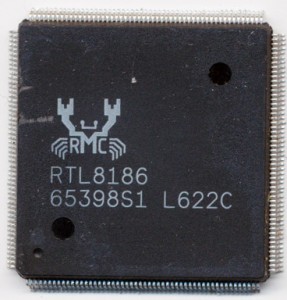
Realtek RTL8186 Lexra LX5280 MIPS with DSP Extentions - 2006

Realtek RTL8186 Lexra LX5280 MIPS with DSP Extensions – 2006

The MIPS architecture was created in 1985 from a project at Stanford University.  It was one of the first licenseable architectures.  A company could buy a license and make their own MIPS architecture processors.  By the 1990’s this had become fairly common and many companies were making MIPS processors, including Performance Semiconductor, IDT, NEC, Toshiba, LSI and more.  In 1992 MIPS Computer Systems, Inc. was bought by SGI, in order to guarantee a supply a continued development of new MIPS designs for SGIs computers.  It did continue to license the design to other companies as well, fostering competition which helped lower prices for SGI.  In 1998 SGI spun off MIPS into its own company once again, as SGI at the time had decided to move towards Intel’s Itanium architecture (this should sound familiar, DEC and the Alpha suffered the same fate).  By 2008 MIPS was losing money and in 2013 what little remained (having used most of their cash to buy, and then sell at a loss Chipidea) of them was bought by Imagination Technologies (makers of the PowerVR line of graphic solutions, used notably in the Apple iPhone’s A4, A5, A6, and likely A7 processors).  But there is a bit more to the story of MIPS, a seemingly small chapter that very well could have changed history and certainly changed the success of MIPS.

In 1997 a small company called Lexra was started. Lexra was a semiconductor Intellectual Property company.  They designed processors and licensed the designs.  What made Lexra different is that they designed and licensed soft-cores.  A soft core is an RTL (Register Transfer Level) model of the processor.  It is usually written and delivered in an HDL (Hardware Descriptive Language) such as Verilog or VHDL and the purchaser may compile it down to whatever actual transistor level hardware they like.  This is exactly how ARM works today, but in 1997 ARM only licensed hard cores, cores already compiled down to the gate level and ready for implementation on a given fab process technology.  This allowed them to have tighter control over the design and its performance, but made integration much harder into other products.  A soft core like Lexra designed enabled rapid integration into a variety of SoCs and other applications.  Lexra’s chosen architecture was MIPS and that is where the story gets interesting.

Read More »

Tags:
, ,

Posted in:
CPU of the Day

November 29th, 2010 ~ by admin

Broadcom’s MIPS Chips

A lot of talk goes on about ARM cores and their increasing use and speed.  While the market penetration, shear speed, and low power of ARM cored devices is certainly amazing its important to not forget that their are other cores in wide use as well, if not as glamorous.  The MIPS architecture was developed at around the same time as ARM (1985) and actually enjoyed success in the market much sooner then ARM did. MIPS continues to be widely used in embedded applications (expecially the MIPS 4000 architecture).

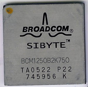
Broadcom Sibyte BCM1250B2K750 - 750MHz dual core MIPS

Broadcom is one of the largest users and producers of MIPS cores devices.  Broadcom recently announced the BRCM5000 MIPSs CPU core. It can issue 2 instructions per cycle and at 40nm runs at at least 1.3GHz (worst case speed).  It should handily clock to 2GHz+ given good process and part selection (the core uses AVS to scale voltage internally to find the perfect voltage/speed combination on a part level basis).  Broadcom chose to not use a multi-core design as a multi-core doubles die area, almost doubles power, but in typical applications does not double performance.  Using a dual-threaded design, on a dual-issue core, does provide almost a doubling of performance, at a minimum of die area.  Die area being a huge concern when the core must be integrated into various products used for mobile devices.  The BRCM5000’s predecessor (the BRCM3000) occupies a mere 1 square mm of die space at 40nm.

Broadcom is not new to the MIPS seen, they have been using them since the 1990’s when Broadcom was founded. Since then they have continually enhanced their products, via internal development, as well as many acquisitions.  Some of the more notable MIPS acquisitions were Sibyte in 2000 who made high-end MIPS network processors and the Xilleon product line from ATI/AMD in 2008 which made Digital TV Processor chips based on the MIPS core.

Just recently Broadcom closed their purchase of Beceem, a company that makes 4G chipsets based on the MIPS core.  MIPS continues to be used not just by Broadcom. Microchip’s PIC32 line is in fact a MIPS R4K processor. Cavium Networks, RMI, Toshiba, NEC, and Sony all continue to use MIPS in a variety of products.   MIPS continues to try to penetrate the smartphone industry, and if at all possible should.  The competition would help keep new innovations coming.

Tags:
,

Posted in:
Uncategorized

April 4th, 2009 ~ by admin

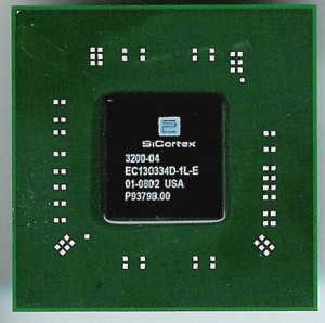
SiCortex: Energy Efficient Super Computing

SiCortex is a supercomputer company, or as they are called today ‘High Performance Computers’ (HPCs). HPCs have traditionally taken vast amounts of room, and vast amounts of power. SiCortex has changed that.  Their fastest  offers 5,832 1.4GFlops 64-bit processors, each dissipating just 900 milliwatts of power. All interprocessor communications logic plus two DDR-2 memory controllers and PCI Express I/O logic are on the same node chip with the multiple processor cores. Complete with its 8 Terabytes of system memory, the SC5832 fits in a single cabinet and only requires around 20 kilowatts of wall power.


SiCortex Node chip

SiCortex Node chip

These nodes, shown above, each contain 6 MIPS64 cores running at 700MHz, a pair of DDR2 memory controllers, gigabit ethernet, an 8xPCI Express controller, and 256k of L2 Cache, quite impressive.

Much thanks to SiCortex for donating this node chip to the museum.