Forgotten Italian CPU – The Genesys B52 MMX
Introduction
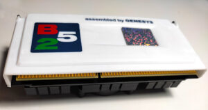 On this site you can read about thousands of processors models. And every year it is more and more difficult to write about some new (old) processors, since everything has been known for a long time. But there are also exceptions to the rule which we love to find. In 2021, I learned about one unusual processor, the information about which I want to share with you. The roots of this processor’s history go back to Italy, in the distant year or 1998. This time just falls on the confrontation between Intel and its second generation Pentium and AMD K6-2 and K6-3 processors. The Cyrix MII processors from Cyrix Corporation, IDT WinChip 2s and Rise mP6s were still going strong as well.
But before we talk about the Genesys B52 MMX processor, we should take a closer look at Intel Pentium II processors in general, as the Italian processor primarily owes its appearance to them.
Intel Pentium II
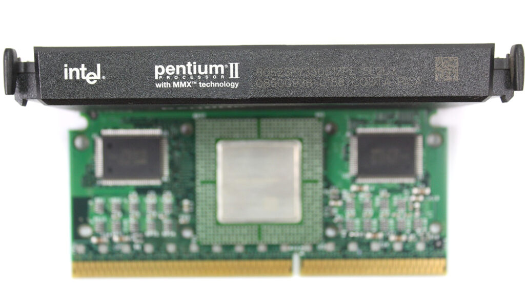
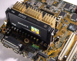 From 1993 to 1997, the Pentium dominated all market segments. Over time, the name of the “Pentium” trademark even grew into a household name (Its all about the Pentiums baby), but with the release of the Pentium II, everything changed. If earlier Intel did not deeply segment the market, there were Pentium Pros for workstations and servers, and for everything else there were various models of Intel Pentium processors, in which, at the end of their domination, Intel added MMX instructions, depriving and thereby putting an end to its server segment. The new slot form factor of the processor, the abandonment of the usual pins and ceramics and further segmentation of the market (using Intel Celeron processors and the new Xeon line) radically changed the further course of development of the history of microprocessors.
 May 7, 1997 saw the light of the first models of Intel Pentium II processors, manufactured on a 350nm process with a core voltage of 2.8 volts. The first models were based on the Klamath core (named after the river by which The CPU Shack is located) core, operating at 233 and 266 MHz. The main differences from the Pentium Pro predecessor it was based on were the L1 cache increased from 16 to 32 Kb, and the presence of a block of SIMD instructions called MMX first introduced on the last P55C processors. Like the Pentium Pro it featured its own L2 cache on the module, but in this case it was 512KB fixed on the same PCB as the processor core, a much cheaper solution then the dual ceramic cavity package of the Pentium Pro.
Before the Pentium II, only the Pentium Pro could boast of its own cache, running at the frequency of the CPU core. But, placing the CPU core and L2 cache on the same substrate was an expensive pleasure even for Intel, and the processors had to be cheaper for better competition, which was getting more and more intense. Intel then made a “wise” decision, as a result of which the Pentium II got a its own L2 cache next to the CPU core This engineering solution significantly reduced the cost of manufacturing processors. BSRAM L2 cache chips were manufactured by Toshiba, SEC and NEC at that time, rather then being made in house by Intel, further easing the cost burdens.
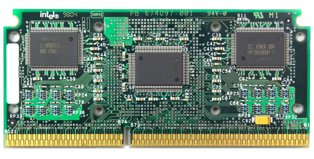
For all models of Pentium II processors, the cache size remained unchanged and equaled 512 KB, while different Pentium Pro models had a cache from 256 to 1024 KB. The L2 cache of the first Pentium II processors consisted of four microcircuits located on both sides of the cartridge processor board and operated at half the core frequency. In addition to the processor core and 4 L2 cache chips, there was also a tag-RAM chip on the cartridge PCB, a total of 6 IC’s.
The tag-RAM size/configuration determines which range of main memory can be cached. For example, if the L2 cache is 256 KB and the tag RAM is 8 bits wide, then this is enough to cache up to 64 MB of main RAM. However, if you add additional RAM in the process, it will not be cached unless you also expand the tag RAM. On Socket 1-3 486 systems, most motherboards allowed adding and modifying additional L2 cache and tag-RAM chips for this purpose. The Pentium Pro had built-in L2 cache and tags capable of caching up to 4GB of main memory, whereas the first Pentium IIs could cache up to 512MB of RAM. This was in part to set them apart from the server oriented Pentium II Xeon which had full speed cache capable of caching 4GB (or 64GB with PSE-36),
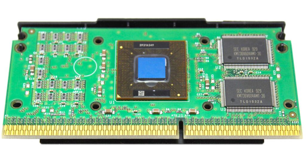
 In January 1998, Intel announced the Pentium II processor, built on a new core, codenamed Deschutes (Another river in Oregon). The processor core was manufactured using the smaller 250nm process, which lowered the operating voltage to 2.0 V, instead of 2.8 V for “Klamath”. The L2 cache of 512 KB still worked at half the core frequency, but it was made in the form of two BSRAM chips located to the side of the processor package. In later modifications of the Pentium II Deschutes core, Intel replaced the tag-RAM chip, thanks to which the processors could cache up to 4 GB of RAM (the 82459AD revision).
The first generation of Intel Celeron processors were based on the “Covington” core were essentially processors on the “Deschutes” core, but without ANY L2 cache. Thanks to this, they had very poor performance, but they overclocked very well, demonstrating the best overclocking figures up to double the nominal clock frequency.
 All overclocking of Pentium II, as a rule, rested on the characteristics of microcircuits used by BSRAM and tag-RAMs. The latter, like the cache, was much disliked voltage rises, and with inept handling, an expensive Pentium II could turn out to be a Celeron “Covington”, if such microcircuits failed.By the way, they warmed up decently on Pentium II processors based on the “Klamath” core so cooling was very important as well. The multiplier in 99% of Pentium II processors was locked (very early production ones were unlocked and Engineering Samples of course), so overclocking was performed by raising the FSB frequency, this being dependent always on the cache and TAG chips installed in that particular processor.
A simple example. In Costa Rica, where Intel has an advanced advanced processor assembly/test factory, which simultaneously assembled high-frequency models with 450 and 300 megahertz. The cartridge and core for these processors are identical (and the multiplier was the same 4.5x as well 66×4.5 for the 300 and 100×4.5 for the 450). The difference was only in the installed cache memory with different speed rating in nanoseconds. Sometimes on the assembly line there was only a fast cache memory capable of operating at a frequency of 225 MHz, intended for models of processors with 450 MHz. In this case, it was also installed on the model with a frequency of 300 MHz, as a result of which they overclocked perfectly.
Genesys B52 MMX CPU
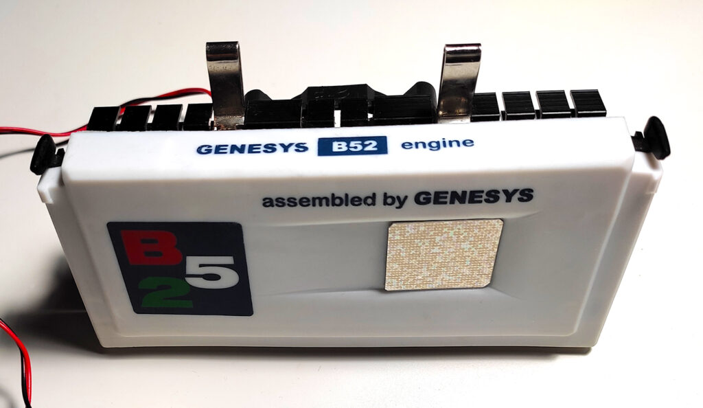
The history of the Italian processor began in the city of Monopoli, in the province of Bari in Italy. In 1998, Italian Marcello Console founded Genesys, which initially employed 10 people. The main idea of the Genesys business was the production of modified Intel Pentium II processors based on the “Deschutes” core, at a much lower price than the Pentium II ones of similar clock speed. Plus a warranty period extended to 3 years and productivity increased by 5% or more. It turns out to be a solid Attraction of Generosity!
Genesys had registered its own domain www.b52mmx.com and is getting ready to implement their processors in ready-made system units. Unfortunately, nothing is known about the manufacturing process, it remains a mystery to this day. There is not so much information on these processors, but let’s try to figure out what these processors were.
Tags:
Intel, Overclocking, Pentium II
Posted in:
CPU of the Day


