AMD 20 Processor Test Board – A Gang of Athlons
Processors are tested at many steps in the manufacturing process. Automated visual inspections are done at several steps during the wafer lithography stage, the individual chips are tested and marked on the wafer before slicing, and then final testing and speed grading during the assembly process.
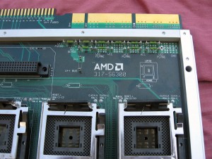
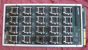
This board is part of that final test stage, It is designed to test Socket A (462) CPU’s, 20 at a time. The board was made by a company called DynaVision in June of 2000, coinciding with the release of AMD’s first Socket A processors. The board would be used in a test machine, and likely manually loaded with up to 20 processors. This cannot be a FULL test of the processor as not all signals are brought out (so it may miss a package defect). All the test, debug and JTAG signals are brought out from each socket, as well as the necessary voltages and CLK signals provided.
A connector by each socket supports, PS_ON, PWERON, ANODE and CATHODE signals, though I am not entirely sure what there are for. Best guess is thermal management. Also next to this is 2 signals labeled TEC1 and TEC2, naming that may suggest Peltier junction cooling.
The board is labeled AMD 317-S6300 and FAB 30-21041B. Fab 30 could suggest AMD’s Dresden Germany Fab, which would make this board even more interesting, as only a very few processors were assembled/tested at the fabs themselves. Most production AMD processors were assembled and tested in Penang, Malaysia (since 1972).
Someone at AMD was certainly intimately familiar with the design and use of this board, and its part in AMD’s success in the market. Now it occupies a few square feet of a wall at the CPU Shack Museum keeping its secrets to itself.
Posted in:
Boards and Systems


