September 2nd, 2023 ~ by admin

SPARCs in Space: The Cobham UT700 Leon3FT Processor

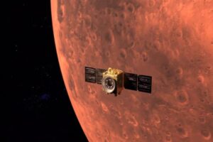
UAE Mars Hope Mission – IR Imager powered by LEON3FT

In the 1990s the ESA began a project to develop their own, open source, easily usable processor for space applications.  Before this the ESA had used mainly MIL-STD-1750A processors, both American made ones, or direct copies their of, such as the Dynex MAS281, a clone of the McDonnel Douglas MDC281.  The ESA explored many different architectures, including the Motorola MC88K RISC process, the MIPS RISC processor, and AMD 29K RISC processor the SPARC, and somewhat oddly, even the National Semiconductor NS32k series processors (which at the time were fairly powerful and used a fair amount in embedded apps).  The SPARC came out of this as the winner.

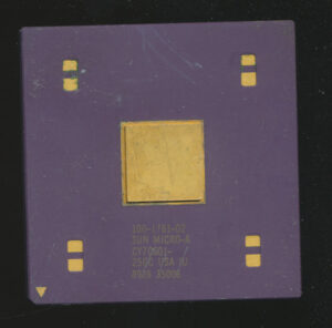
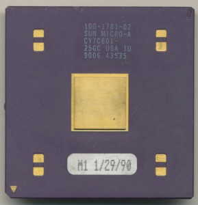
Cypress CY7C601 SPARC Processor. The basis for the ERC32

At the time the SPARC was a pretty widely used processor, and was being developed by multiple companies.  It was defined as an architecture, and various companies could implement it how they saw fit, in various technologies.  This is very much how the 1750A architecture was made to be as well.  Considering this, the only two really viable architectures that wouldn’t (at that time) have been a sole source item, were the MIPS and the SPARC, both were used and made by many companies, but SPARC it was.

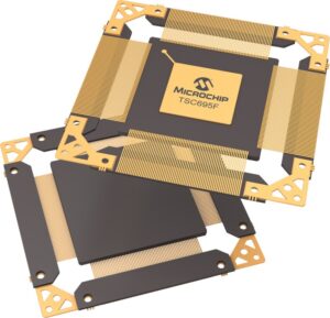
Atmel TSC695 – ERC32 Single Chip SPARC V7 – Still in production

The first implementation was the ERC32 released in 1995, a early SPARC V7 3-chip implementation typically made on a  0.8u process.  These were decent, but took 3 chips, were limited to 20MHz due to memory interface limitations, and were not particularly scalable.  The ERC32 did fly to space, and was used on the ISS as one of the main control computers, as well as 10 other missions including the ESAs ATV resupply vehicles for the ISS.  By 1998 the ERC32 was shrunk to 0.6u allowing it to be integrated onto a single chip (the Atmel TSC695).  This became the standard ESA processor as well as being used by other nations, including China, Israel, India and even NASA.

By the year 2000 the SPARC V7 architecture was rather long in the tooth, having been originally designed back in the 1980’s.  The decision was made to upgrade to SPARC V8.  SPARC V8 added integer multiply/divide instructions, as well as expanded the floating point from 80-bit to 128-bit.  SPARC V8 became the basis for the IEEE 1754-1994 standard for what a 32-bit processor must do.  This was important as it made a very clear definition for software as well, ESA wanted a processor whose support was very well known, and very well defined.  The SPARC V8 implementation became the LEON (for Lion) processor.  These used a 5-stage pipeline (Fetch, Decode, Execute, Memory, Write) and were made on a 0.35u process delivering around 50MIPS at 0.5W. It used around 100,000 gates on a 30mm2 die and was a fully Fault Tolerant design (unlike the ERC32).  It was rated to handle 300Krad of ionizing radiation without upset.

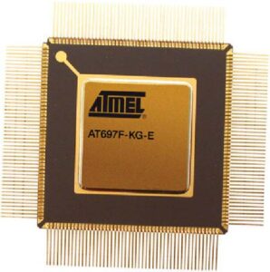
Atmel AT697 LEON2

LEON2 was a fairly similar deign, it moved the MUL/DIV instructions into hardware (instead of emulating them on LEON1) and reduced the feature size down to 0.18u.  It also added many on chip peripherals, such as a PC133 SDRAM controller (with Error detection/Correction) as well as a AMBA bus.  It took around 0.6W at 100MIPS though some implementation saw speeds of up to 120MIPS at 0.3W).  LEON2 saw use on many missions, including the camera controller for the Venus Express mission and the BepiColombo mission to Mercury. LEON2 was designed as a single function processor, but in the real world was often being used as a SoC (System on a Chip).

This led to the development of the LEON3 in 2004.  It was originally made on a slightly LARGER process of 0.20u.  It ran at around 150MIPS at 0.4W.  Its biggest upgrades were moving from a 5-stage pipeline to a 7–stage pipeline (Fetch, Decode, Register Access, Execute, Memory, Exception, Write) as well as supporting multiprocessing.  In realization of the actual use cases the LEON processors were seeing (as SoCs rather then as single processors) the LEON3 added a large array of peripherals.  This included Spacewire, MIL-STD-1553  interfaces, DDR RAM controllers, USB controllers, 1G Ethernet MAC, and much more.  All stuff that originally had to be added on to previous systems was now on chip.

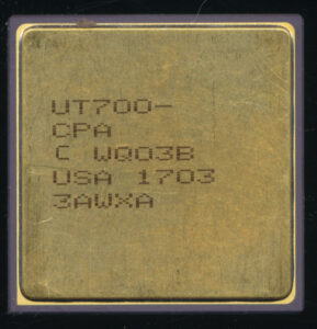
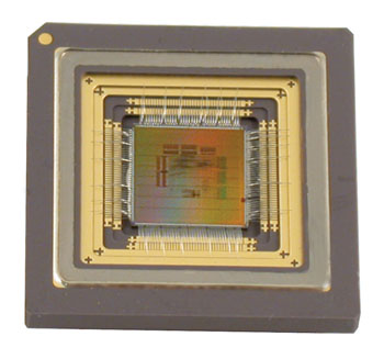
Cobham UT700 Fault Tolerant SPARC V8 LEON3FT

The entire design was good for 400MHz on a 0.13u process and used around 25,000 gates.  Like the LEONs before it, the LEON3 was designed as a synthesizable device.  You could implement the entire core in your on ASIC or FPGA, or buy an FPGA off the shelf already programmed as one (Aeroflex offers this option). You could also buy ready made processors implementing it, much like any other CPU.  Cobham (now known as CAES Cobham Advanced Electronic Solutions) offers the UT700.  The UT700 is a 166MHz processor implementing the full LEON3FT design.  The ‘FT’ stands for Fault Tolerant, and adds a lot of error checking and correcting features on top of the base LEON3 design.  Every bit of RAM on chip, from registers, to cache has error detection and correction.  The UT700 includes 16K of Instruction and Data cache on chip as well as all the usual memory controllers and communication interfaces of the LEON3.  It runs at 1.2-1.8V and and max performance dissipates 4W.

The LEON3FT powers the European Galileo navigation satellites, and many others, including the French Spot-6 Earth Observation craft.  They also power each of the Iridium-NEXT communications satellites that began launching in 2017


Posted in:
CPU of the Day

June 5th, 2017 ~ by admin

SiFive FE310: Setting The RISC Free

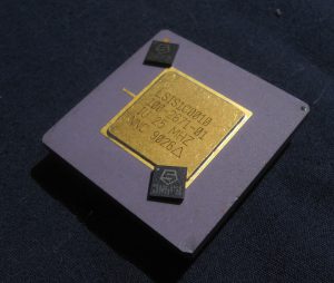
SiFive FE310 RISC-V Processor. Early LSI SPARC Processor for size comparison. Both are based on U.C. Berkeley RISC designs.

The idea of RISC (Reduced Instruction Set Computer) processors began in education, specifically University of California, Berkeley in the early 1980’s, and it was out universities that some of the most famous RISC designs came.  MIPS, still in use today, started life as a project at Stanford University, and SPARC, made famous by Sun, and now made by Oracle and Fujitsu, started life as a Berkeley University project.  Universities have continued to work with RISC architectures, for research and teaching.  The simplicity of RISC makes them an ideal educational tool for learning how computers/processors function at their basic levels.

By the late 1980’s RISC had begun to become a commercial revolution, with nearly every player having their own RISC design.  AMD (29k), Intel (i960), HP (PA-RISC), Weitek (XL8000), MIPS, SPARC, ARM, Hitachi (SH-RISC), IBM (POWER), and others offered their take on the RISC design.  Most were proprietary, while a few were licenseable, none were open architectures for anyone to use.

Unfortunately, outside of the university, RISC processors are not as simple.  The architectures, and their use may be, but licensing them for the design is not.  It can often take more time and effort to license a modern RISC processor then it does to actually implement it.  The costs to use these architectures,both in time and money often prohibit their very use.

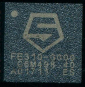
SiFive FE310 – Sample Donated by SiFive. Full 32-bit RISC on a 7.2mm2 die in a ~36mm2 package

It is out of this that SiFive began.  SiFive was founded by the creators of the first commercially successful open RISC architecture, known as RISC-V.  RISC-V was developed at Berkeley, fittingly, in 2010 and was designed to be a truly useful, general purpose RISC processor, easy to design with, easy to code for, and with enough features to be commercially useful, not limited to the classroom.  It is called the RISC-V because it is the fifth RISC design developed at Berkeley, RISC I and RISC II being designed in 1981, followed by SOAR (Smalltalk On A RISC) in 1984 and SPUR (Symbolic Processing Using RISC) in 1988.  RISC-V has already proved to be a success, it is licensed freely, and in a way (BSD license) that allows products that use it to be either open, or proprietary.  One of the more well known users is Nvidia, which announced they are replacing their own proprietary FALCON processors (used in their GPUs and Tegra processors) with RISC-V.  Samsung, Qualcomm, and others are already using RISC-V.  These cores are often so deeply embedded that their existence goes without mention, but they are there, working in the background to make whatever tech needs to work, work.

The RISC-V architecture supports 122 instructions, 98 of which are common to almost all prior RISC designs and 18 common to a few.  Six completely new instructions were added to handle unique attributes of the architecture (using a 64-bit Performance Register in a 32-bit arch.) and to support a more powerful sign-injection instruction (which can be used for absolute value, among other things). It uses 31 32-bit registers (Register 0 is reserved for holding the constant ‘0’) with optional support for 32 floating point registers.  True to the RISC design, it is a pure Load/Store processor, the only accesses to memory are via the Load/Store instructions.

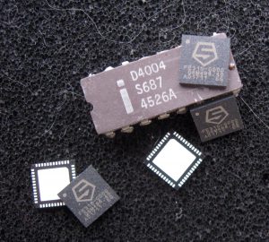
Intel 4004 with 5 SiFive RISC Processors. The 4004 was meant for a calculator. The FE310 is meant for whatever your mind may dream up.

SiFive is unique among RISC IP companies.  They not only license IP but also sell processors and dev boards.  The FE310 (Freedom Everywhere 310) is a 320MHz RISC-V architecture with 16K of I-cache and 16K of scratchpad RAM fabbed by TSMC on a 180nm process. Even on this process, which is now a commodity process, the FE310’s efficient design results in a die size of only 2.65mm x 2.72mm.  On a standard 200mm wafer , this results in 3500 die per wafer, greatly helping lower the cost.  Its an impressive chip, and one that is completely open source.  What is more impressive is licensing SiFive cores, it is a simple and straightforward process.  The core (32 bit E31 or 64-bit E51) can be configured on SiFive’s site, with pricing shown as you go.  The license is a simple 7 page document that can be signed and submitted online.  Pricing starts at $275,000 and is a one time fee, there are no continuing royalty payments.  The entire process can be completed in a week or less.

In comparison, ARM, the biggest licensor of RISC processors, does not publish pricing, charges 1-2% royalties on every chip made, and has a license process that can take over a year.  The base fees start at around $1 million and go into the 10’s of millions, depending on how you want to use the IP, where it will be, and for how long.  For many small companies and users this is simply not feasible, and it is these smaller users that SiFive wishes to work with.  Licensing a processor for the next great tech, should not be the hurdle that it has become.  Many great ideas never make it to fruition due to these roadblocks.  We look forward to finding SiFive processors and cores in all sorts of products in the future.

Thanks to SiFive for their generous donation of several FE310 processors to the CPU Shack Museum.

Tags:
, , , ,

Posted in:
CPU of the Day
July 3rd, 2016 ~ by admin

Juno Joins Jupiter: And Brings Some Computers For The Trip

Juno - RAD750 Powered Mission to Jupiter

Juno – RAD750 Powered Mission to Jupiter

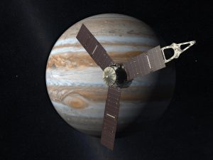
NASA’s Juno mission to Jupiter arrives in just about a day, after a 5 year journey that began in August of 2011 aboard an Atlas V rocket.  The Juno mission is primarily concerned with studying the magnetic fields, particles, and structure of Jupiter.  Finding out how Jupiter works, and what its core is made of are some of Juno’s goals.  None of the experiments need a camera, but NASA decided, in the interest of public outreach and education, that if you are going to spend $1 billion to send a probe to Jupiter, it probably should have a camera.  Energetic particle detectors, Magnetometers, and Auroral Mappers are great for science, but what the public is inspired by is pretty pictures of wild and distant worlds.

Juno is powered by a now familiar computer, the BAE RAD750 PowerPC radiation hardened computer.  It operates at up to 200MHz (about the processing power of a mid 1990’s Apple Computer) and includes 256MB of Flash memory and 128MB of DRAM.  It (and the other electronics) are encased in a 1cm thick titanium radiation vault.  Flying in a polar orbit around Jupiter, Juno will experience intense radiation and magnetic fields.  The probe is expected to encounter radiation levels in the order of 10Mrads+.  The vault limits this to 25krads, within what the electronics can handle.  It should be noted that a dose of 10krads is fatal in most cases.  This intense of radiation will degrade the prober, even with shielding, resulting in a mission life of only 37 orbits (a little over a year) before the probe will be gracefully crashed into Jupiter.

Read More »

January 20th, 2014 ~ by admin

Welcome Back Rosetta: The Dynex MAS31750 Awakens

Rosetta Comet Chaser - Dynex 1750

Rosetta Comet Chaser – Dynex 1750

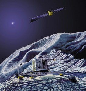
The ESA’s comet chaser Rosetta has just today awoken from a long deep sleep on its comet chasing (and landing) mission.  The solar powered spacecraft was launched back in 2004.  It is based on the Mars Mariner II (itself based on the Voyager and Galileo) spacecraft design of the early 1990s (when the mission was first conceived.)  Main differences include using very large solar arrays versus a RT (Radioisotope Thermal Generator) and upgraded electronics.

In order to conserve power on its outward loop (near Jupiter’s orbit) most all systems were put to sleep in June of 2011 and a task set on the main computer to waken the spacecraft 2.5 years later and call home.  The computer in charge of that is powered by a Dynex MAS31750 16-bit processor running at 25MHz, based on the MIL-STD-1750A architecture.

A reader recently asked why such an old CPU design is still being used rather then say an x86 processor.  As mentioned above the Rosetta design was began in the 1990’s, the 1750A was THE standard high reliability processor at the time, so it wasn’t as out of date as it is now that its been flying through space for 10 years (and 10 years in the clean room).  The 1750A is also an open architecture, no licenses are or were required to develop a processor to support it (unlike x86). Modern designs do use more modern processors such as PowerPC based CPUs like the RAD750 and its older cousin the RAD6000.  Space system electronics will always lag current tech due to the very long lead times in their design (it may be 10 years of design n the ground before it flies, and the main computer is selected early on).  x86 is used in systems with 1) lots of power, and 2) somewhat easily accessible.  Notably the International Space Station and Hubble.  x86 was not designed with high reliability and radiation tolerance in mind, meaning other methods (hardware/software) have to be used to ensure it works in space.

Currently the ESA designs with an open-source processor known as the LEON, which is SPARC-V8 based.

January 18th, 2013 ~ by admin

CPU of the Day: Cypress CY7C601 25MHz SPARC

Cypress CY7C601-25GC

Cypress CY7C601-25GC – First package with heatspreader – Omitted on later versions

In Mid-1987 Sun Microsystems (now owned by Oracle) released the SPARC (Scalable Processor ARChitecture)  processor architecture to be used in their computers (replacing the 68k based systems they had previously used).  The SPARC was designed from the outset to be an open architecture, allowing manufactures to license and built processors that implemented it using whatever technology they wished.  The goal of this was to 1) build a large SPARC ecosystem and 2) keep prices in check by fostering competition among manufacturers.  The SPARC is still used today by Oracle, Fujitsu, the European Space Agency and others, owing largely to its design as an open architecture from the very beginning.

The first version was made by Fujitsu on a 20,000 gate array at 1.2 micron and ran at 16.6MHz.  In July 1988 Cypress  (later to be spun off as Ross and make the famous HyperSPARC line) announced the CY7C601.  This was the fastest implementation of the SPARC at the time.  It was made on 0.8u CMOS process and contained 165,000 transistors, dissipating around 3.3Watts.  As was typical of many processor designs of the time, it was an integer only processor, requiring a separate chip (the CY7C602) for floating point work.  In September of 1988, Cypress cross licensed the ‘601 to Texas Intruments in exchange for rights to the 8847 floating point processor.  This was mainly to appease one of Cypress main customers who demanded that a second source for the ‘601 chips be available, a demand more common in the 1970s then in 1988 but Cypress obliged.  Cyrpress also gained the rights to make the next generation SPARC processor that TI was developing.  TI would go on to make many SPARC processors, and continued to be the primary fab for Sun up through the SPARC T2 Plus in 2008.  Oracle now used TSMC to fab the T3 and T4 SPARC processors.

Tags:
, , ,

Posted in:
CPU of the Day

July 27th, 2009 ~ by admin

The other Atmel: Radiation Hardened Sparc CPU’s

When you think of Atmel what do you typically thing? High Speed 8051 microcontrollers and AVR RISC processors.  Maybe the occasional EEPROM. But there is another side of Atmel.

Atmel AT697F Rad-Hard SPARC

Atmel AT697F Rad-Hard SPARC

Atmel also makes a line of radiation hardened space qualified SPARC CPU’s. These are used extensively by the  European Space Agency and other satellite builders.  Atmel just released anew one too. The AT697F, a revision of the AT697E. What can it do? well oits a full 32bit SPARC V8 core, running at 100MHz (90MIPS). Its made on 0.18u which is very impressive for a space based processors. Most of Atmels other designs are basing on a half micron process.

A larger process like half a micron gives increased radiation resistance, but at the expense of speed. At 0.18u Atmel has got the speed up to 100MHz, AND increased radiation tolerance to 300krads.  To put that in perspective, a dose of only 1 krad (1000 rems) will kill you 99% of the time so these processors can continue to function at over 300 times that.

Source:  EE Product Center