

 |
 |
 |
| home | about | pictures | reference | trade | links |
How a CPU Microprocessor Is Made
This is a quick tutorial to help you understand how microprocessors and other integrated circuits are made, or 'fabbed.' Starting from a chunk of silicon and resulting in a device with millions and millions of transistors that now run almost everything in your life.
Making the Wafer
CPUs are made mostly of an element called silicon. Silicon is rather common in earths crust and is a semiconductor. This means that depending on what materials you add to it, it can conduct when a voltage is applied to it. It is the 'switch that makes a CPU work. Modern CPUs literally contain millions transistors.
![]()
Raw silicon
The first stage in making a CPU is to make the wafers that they are built
on. This process begins with the melting of polysilicon, together with minute
amounts of electrically active elements such as arsenic, boron, phosphorous
or antimony in a quartz crucible (a container that won't melt at high temperatures).

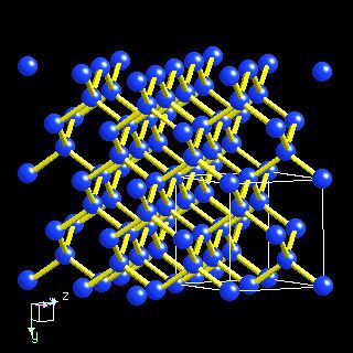
Silicon is a simple FCC Lattice (Face Centered Cubic)
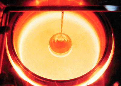
Once the melt has reached the desired temperature, we lower a silicon seed crystal, or "seed" into the melt. The melt is slowly cooled to the required temperature, and crystal growth begins around the seed. As the growth continues, the seed is slowly extracted or "pulled" from the melt. As the the ingot is pulled it is slowly rotated. This is done to help normalize any temperature variations in the melt. The temperature of the melt and the speed of extraction govern the diameter of the ingot, and the concentration of an electrically active element in the melt governs the electrical properties of the silicon wafers to be made from the ingot. This is a complex, proprietary process requiring many control features on the crystal-growing equipment. The crystals naturally tend to a circular shape due to the crystal structure itself, and the surface tension on the liquid.

6" ingot is drawn out of the melt. This process can take several hours.
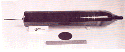
This results in a large ingot that looks like this:

To be useful the ingot must be very pure. The ends and edges are the areas
of highest impurities (this is due to annealing) so the ends are cut off and
the edges are ground down so the ingot is the proper diameter.
Next the wafers are cut from the ingot. They are usually cut 1-2mm thick
with a fast wire saw. The edges of these wafers are then rounded to prevent
chipping and edge cracks. The wafers are then ground and polished both chemically
and mechanically to produce a very flat, mirror like surface.

Wafers may then be heated to help remove any defects. (annealing)

The wafers are then inspected with a laser to find any surface defects.

A single crystal layer (epilayer) may then be added to the surface of the
wafer.
The wafer is now ready for etching.
Continue to: Etching - Making
of the Microprocessor
Making of Microprocessors 1
- 2 - 3 - 4